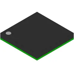
이미지는 참조용만
10M50SAE144C8G
IC FPGA 101 I/O 144EQFP
- 제조업체
- Mfr.부분 #10M50SAE144C8G
- 패키지 144-LQFP
- 데이터시트
- 재고 있음5222
100% 원래 &새로운
배송 준비 24 시간
365 일 보장
RFQ 및더 많은 할인
사양
| Package | Tray |
| Series | MAX® 10 |
| ProductStatus | Active |
| NumberofLABs/CLBs | 3125 |
| NumberofLogicElements/Cells | 50000 |
| TotalRAMBits | 1677312 |
| NumberofI/O | 101 |
| Voltage-Supply | 2.85V ~ 3.465V |
| MountingType | Surface Mount |
| OperatingTemperature | 0°C ~ 85°C (TJ) |
| Package/Case | 144-LQFP Exposed Pad |
개요
Description
It supports a variety of interfaces, including GPIO, SPI, and I2C, making it versatile for different designs. The 10M50SAE144C8G also includes built-in ADCs, digital signal processing capabilities, and various memory options, enabling designers to implement complex algorithms and functionalities efficiently.
Additionally, the FPGA can be programmed using Intel's Quartus Prime software, which facilitates design and simulation, making it accessible for both novice and experienced developers. The combination of low power consumption and high configurability makes the 10M50SAE144C8G an attractive choice for applications requiring customizable hardware solutions.
Features
1. Logic Elements: Offers 50,000 logic elements, allowing for complex designs.
2. I/O Pins: Provides up to 144 user-configurable I/O pins for versatile connectivity.
3. Memory: Includes embedded memory blocks, supporting up to 1.2 Mb of RAM.
4. Analog Functionality: Features integrated analog-to-digital converters (ADCs) for mixed-signal applications.
5. Low Power: Designed for low power consumption, making it suitable for battery-operated devices.
6. Single Supply Voltage: Operates at a single supply voltage (3.3V), simplifying power management.
7. JTAG Support: Includes JTAG for easy configuration and debugging.
8. Flash Memory: Integrated flash memory allows for non-volatile storage of the configuration bitstream.
This FPGA is ideal for applications in industrial, automotive, and consumer electronics, offering flexibility and ease of use in design.
Package
Pinout
The key functions of the 10M50SAE144C8G include:
- Logic Elements (LEs): Configurable logic blocks for implementing combinatorial and sequential logic.
- Embedded Memory: Supports RAM and ROM configurations for on-chip data storage.
- I/O Pins: Configurable for various protocols such as LVTTL, LVCMOS, and others, allowing interfacing with external devices.
- DSP Blocks: For high-performance arithmetic operations.
- PLL and Clock Management: Integrated phase-locked loops for clock generation and management.
Overall, this FPGA is suitable for applications in communications, automotive, industrial control, and other digital processing tasks.
Manufacturer
Application
Equivalent
배송
배송 방법We
DHL, FedEx, TNT, UPS 또는 선택한 다른 운송업체를 통해 글로벌 배송 서비스를 제공합니다.
배송 요금 참조 (DHL/FedEx):
DHL은: 배송 비용은 $25-$45 (0.5kg)에서 2-5 영업일의 추정적 배달 시간이 있습니다.
FedEx는: 배송 비용은 $25-$40 (0.5kg)에서 3-7 영업일의 추정적 배달 시간을 가지고 있습니다.
UPS는: 배송 비용은 $25-$45 (0.5kg)에서 3-7 영업일의 추정적 배달 시간을 가지고 있습니다.
TNT는: 배송 비용은 $25-$65 (0.5kg)에서 3-7 영업일의 추정적 배달 시간을 가지고 있습니다.
EMS는: 배송 비용은 $30-$50 (0.5kg)에서 7-15 영업일의 추정적 배달 시간을 제공합니다.
등록된 항공우편: 배송 비용은 $2-$4 (0.1kg), 예상 배달 시간 5-20 영업일.
지불
Payment Methods
지불 기간은 100% 사전 지불입니다.
현재, 우리는 아래 지불 방법만 받아들입니다.:
1. PayPal
2. 신용/직불 카드
3. 전선 전송
비슷한
-
![MX25L3233FM1I-08Q]() MX25L3233FM1I-08Q
Macronix
-
![MX25V1635FZNQ03]() MX25V1635FZNQ03
Macronix
-
![MX25V2033FM1I]() MX25V2033FM1I
Macronix
-
![MX25L8035EM2I-10G]() MX25L8035EM2I-10G
Macronix
-
![MX25L25673GMI-08G]() MX25L25673GMI-08G
Macronix
-
![MX29GL512FHXFI-11G]() MX29GL512FHXFI-11..
Macronix
-
![MX25L2006EM1I-12G]() MX25L2006EM1I-12G
Macronix
-
![MX25U6435FM2I-10G]() MX25U6435FM2I-10G
Macronix
-
![MX25L12833FM2I-10G]() MX25L12833FM2I-10..
Macronix
-
![MX25L12833FZ2I-10G]() MX25L12833FZ2I-10..
Macronix
-
![MX25L12833FZNI-10G]() MX25L12833FZNI-10..
Macronix
-
![MX25L12835FZ2I-10G]() MX25L12835FZ2I-10..
Macronix