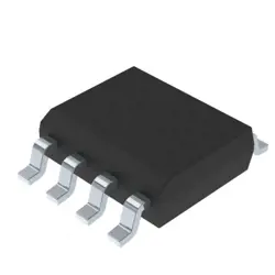
이미지는 참조용만
AD711JR
IC OPAMP JFET 1 CIRCUIT 8SOIC
- 제조업체
- Mfr.부분 #AD711JR
- 패키지
- 데이터시트
- 재고 있음2055
100% 원래 &새로운
배송 준비 24 시간
365 일 보장
RFQ 및더 많은 할인
사양
| Part Status | Obsolete |
| Amplifier Type | J-FET |
| Number of Circuits | 1 |
| Slew Rate | 20V/µs |
| Current - Input Bias | 15 pA |
| Voltage - Input Offset | 300 µV |
| Current - Supply | 2.5mA |
| Current - Output / Channel | 25 mA |
| Voltage - Supply Span (Min) | 9 V |
| Voltage - Supply Span (Max) | 36 V |
| Operating Temperature | 0°C ~ 70°C |
| Mounting Type | Surface Mount |
| Package / Case | 8-SOIC (0.154", 3.90mm Width) |
| Supplier Device Package | 8-SOIC |
| Base Product Number | AD711 |
| -3db Bandwidth | 4 MHz |
개요
Description
Key specifications include a typical offset voltage of 100 µV, a bandwidth of 3 MHz, and a gain bandwidth product of 1 MHz. Its low noise characteristics enhance performance in sensitive applications, such as instrumentation and audio processing. The AD711JR is available in various package types, providing options for different space and thermal requirements.
Engineered for robustness, it is often used in medical devices, industrial controls, and data acquisition systems. Overall, the AD711JR is favored for its reliability and precision in critical electronic applications.
Features
1. Low Offset Voltage: Typically around 100 µV, ensuring accurate signal amplification.
2. Low Noise: With a voltage noise density of 1.6 nV/√Hz, it minimizes signal interference.
3. Wide Supply Voltage Range: Operates from ±2 V to ±15 V, allowing flexibility in various circuit designs.
4. High Slew Rate: Approximately 0.5 V/µs, enabling fast signal processing.
5. High Gain: This op-amp provides a large open-loop voltage gain of up to 100 dB, ensuring effective signal amplification.
6. High Input Impedance: Typically around 1 MΩ, reducing the loading effect on preceding stages.
7. Low Input Bias Current: About 100 pA, making it ideal for high-impedance sensor applications.
Overall, the AD711JR is well-suited for precision data acquisition, instrumentation, and signal conditioning tasks.
Package
Pinout
1. Offset Null - Pin 1: Used for offset voltage adjustment.
2. Inverting Input (V-) - Pin 2: Input for the inverting signal.
3. Non-Inverting Input (V+) - Pin 3: Input for the non-inverting signal.
4. Output - Pin 6: The output of the amplifier.
5. Supply Voltage (V-) - Pin 4: Negative supply voltage connection.
6. Supply Voltage (V+) - Pin 7: Positive supply voltage connection.
7. NC (No Connection) - Pin 5: Not connected, typically left open.
8. NC (No Connection) - Pin 8: Not connected, typically left open.
This op-amp is designed for high-speed applications and provides low offset voltage and low noise, making it suitable for precision signal processing tasks.
Manufacturer
Application
Equivalent
배송
배송 방법We
DHL, FedEx, TNT, UPS 또는 선택한 다른 운송업체를 통해 글로벌 배송 서비스를 제공합니다.
배송 요금 참조 (DHL/FedEx):
DHL은: 배송 비용은 $25-$45 (0.5kg)에서 2-5 영업일의 추정적 배달 시간이 있습니다.
FedEx는: 배송 비용은 $25-$40 (0.5kg)에서 3-7 영업일의 추정적 배달 시간을 가지고 있습니다.
UPS는: 배송 비용은 $25-$45 (0.5kg)에서 3-7 영업일의 추정적 배달 시간을 가지고 있습니다.
TNT는: 배송 비용은 $25-$65 (0.5kg)에서 3-7 영업일의 추정적 배달 시간을 가지고 있습니다.
EMS는: 배송 비용은 $30-$50 (0.5kg)에서 7-15 영업일의 추정적 배달 시간을 제공합니다.
등록된 항공우편: 배송 비용은 $2-$4 (0.1kg), 예상 배달 시간 5-20 영업일.
지불
Payment Methods
지불 기간은 100% 사전 지불입니다.
현재, 우리는 아래 지불 방법만 받아들입니다.:
1. PayPal
2. 신용/직불 카드
3. 전선 전송
비슷한
-
![MX25V1635FZNI]() MX25V1635FZNI
Macronix
-
![MX25V16066M2I02]() MX25V16066M2I02
Macronix
-
![MX25L25673GMI-10G]() MX25L25673GMI-10G
Macronix
-
![MX25U25643GZNI00]() MX25U25643GZNI00
Macronix
-
![MX25R1635FZUIH0]() MX25R1635FZUIH0
Macronix
-
![MX25L12835FZ2I-10G]() MX25L12835FZ2I-10..
Macronix
-
![MX29LV160DTTI-70G]() MX29LV160DTTI-70G
Macronix
-
![MX29F040CQI-70G]() MX29F040CQI-70G
Macronix
-
![MX25L25645GXDI-08G]() MX25L25645GXDI-08..
Macronix
-
![MX29F040CTI-70G]() MX29F040CTI-70G
Macronix
-
![MX25L1006EMI-10G]() MX25L1006EMI-10G
Macronix
-
![MX66U1G45GMI00]() MX66U1G45GMI00
Macronix