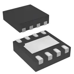
이미지는 참조용만
AD9837BCPZ
Clock Synthesizer / Jitter Cleaner Low Cost DDS IC.
- 제조업체
- Mfr.부분 #AD9837BCPZ
- 패키지
- 데이터시트
- 재고 있음9319
100% 원래 &새로운
배송 준비 24 시간
365 일 보장
RFQ 및더 많은 할인
사양
| Standard Pack Qty | 5000 |
개요
Description
Key features include a serial interface for easy programming, low power consumption (typically under 100 µA), and the capability to output signals in a wide frequency range, making it suitable for various applications like signal generation in communication systems, instrumentation, and audio applications.
It supports frequency modulation and phase modulation, allowing for versatile waveform manipulation. Integration into existing systems is facilitated by its compact size and standard package options. The AD9837BCPZ is ideal for developers needing an efficient and flexible waveform generator in embedded systems.
Features
1. Frequency Range: It can generate sine, triangular, and square waveforms from 0.1 Hz to 12.5 MHz.
2. Resolution: Offers 28-bit frequency tuning resolution, ensuring precision in frequency generation.
3. Low Power Consumption: Operates with a supply voltage of 2.3V to 5.5V and consumes minimal power, making it suitable for battery-operated devices.
4. Programmable Waveforms: Users can easily program frequency and waveform type via a serial interface (SPI).
5. Integrated DAC: Contains a built-in digital-to-analog converter for direct output of the desired waveforms.
6. Output Amplitude Control: Features programmable output amplitude, allowing for flexibility in signal strength.
7. Phase Modulation: Supports phase modulation capabilities for advanced signal generation.
8. Compact Package: Available in a 20-lead LFCSP package, facilitating easy integration into various applications.
These features make the AD9837BCPZ ideal for applications such as signal generation, communication systems, and audio synthesis.
Package
Pinout
1. VDD: Power supply (typically +3.3V).
2. GND: Ground.
3. SCLK: Serial clock input for data transfers.
4. SDATA: Serial data input for programming the device.
5. FSYNC: Frame sync input to latch data into the device.
6. RESET: Active-low reset input.
7. MCLK: Master clock input (reference frequency).
8. FQ_UD: Frequency update pin for updating frequency registers.
9. SINE_OUT: Sine wave output.
10. TRIANGLE_OUT: Triangle wave output.
11. PA0, PA1: Programmable output pins.
12. VOUT: Output voltage.
13. ADJUST: Used for output amplitude adjustment.
Additional pins are reserved for specific functions or may be unconnected. The AD9837BCPZ is designed for generating precise frequency outputs suitable for various applications like signal generation and waveform synthesis.
Manufacturer
Application
Equivalent
배송
배송 방법We
DHL, FedEx, TNT, UPS 또는 선택한 다른 운송업체를 통해 글로벌 배송 서비스를 제공합니다.
배송 요금 참조 (DHL/FedEx):
DHL은: 배송 비용은 $25-$45 (0.5kg)에서 2-5 영업일의 추정적 배달 시간이 있습니다.
FedEx는: 배송 비용은 $25-$40 (0.5kg)에서 3-7 영업일의 추정적 배달 시간을 가지고 있습니다.
UPS는: 배송 비용은 $25-$45 (0.5kg)에서 3-7 영업일의 추정적 배달 시간을 가지고 있습니다.
TNT는: 배송 비용은 $25-$65 (0.5kg)에서 3-7 영업일의 추정적 배달 시간을 가지고 있습니다.
EMS는: 배송 비용은 $30-$50 (0.5kg)에서 7-15 영업일의 추정적 배달 시간을 제공합니다.
등록된 항공우편: 배송 비용은 $2-$4 (0.1kg), 예상 배달 시간 5-20 영업일.
지불
Payment Methods
지불 기간은 100% 사전 지불입니다.
현재, 우리는 아래 지불 방법만 받아들입니다.:
1. PayPal
2. 신용/직불 카드
3. 전선 전송
비슷한
-
![MX25L3233FZBI-08Q]() MX25L3233FZBI-08Q
Macronix
-
![MX25V1635FZNI]() MX25V1635FZNI
Macronix
-
![MX29F400CBTI-70G]() MX29F400CBTI-70G
Macronix
-
![MX25V4035FZUI]() MX25V4035FZUI
Macronix
-
![MX25V2033FM1I]() MX25V2033FM1I
Macronix
-
![MX25V16066M1I02]() MX25V16066M1I02
Macronix
-
![MX25V16066M2I02]() MX25V16066M2I02
Macronix
-
![MX25L25673GMI-10G]() MX25L25673GMI-10G
Macronix
-
![MX25U3232FZBI02]() MX25U3232FZBI02
Macronix
-
![MX25L6433FM2I-08G]() MX25L6433FM2I-08G
Macronix
-
![MX25U6435FM2I-10G]() MX25U6435FM2I-10G
Macronix
-
![MX25L25645GXDI-08G]() MX25L25645GXDI-08..
Macronix