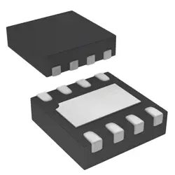
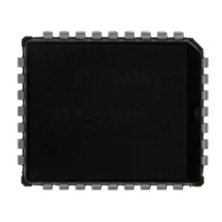
이미지는 참조용만
AD9910BSVZ
IC DDS 1GHZ 14BIT 100TQFP
- 제조업체
- Mfr.부분 #AD9910BSVZ
- 패키지 TQFP-100
- 데이터시트 AD9910BSVZ DataSheet
- 재고 있음7448
100% 원래 &새로운
배송 준비 24 시간
365 일 보장
RFQ 및더 많은 할인
사양
| Package | Tray |
| ProductStatus | Active |
| Resolution(Bits) | 14 b |
| Masterfclk | 1 GHz |
| TuningWordWidth(Bits) | 32 b |
| Voltage-Supply | 1.8V, 3.3V |
| OperatingTemperature | -40°C ~ 85°C |
| MountingType | Surface Mount |
| Package/Case | 100-TQFP Exposed Pad |
개요
Description
Key features include a 14-bit DAC (digital-to-analog converter) for high output resolution, a programmable output frequency, and the ability to modulate amplitude, frequency, and phase. The AD9910 supports various modulation schemes, making it versatile for signal generation tasks.
It interfaces with microcontrollers and FPGAs through a serial port interface (SPI), allowing for easy integration into existing systems. The chip also includes built-in features like a phase accumulator and a frequency tuning word to facilitate precise tuning.
Overall, the AD9910BSVZ is an essential component for modern electronic systems that require accurate and flexible signal generation capabilities.
Features
1. Frequency Range: Capable of generating frequencies up to 1 GHz.
2. Resolution: 14-bit digital-to-analog converter (DAC) for high signal fidelity.
3. Phase Offset: 14-bit phase modulation capabilities for precise phase control.
4. Output Modes: Supports various output modes, including single-tone and frequency sweep.
5. Integrated Features: Built-in digital frequency modulation and a programmable output stage.
6. Low Phase Noise: Enhanced spectral purity with low phase noise characteristics.
7. Flexible Interface: Serial port interface for easy control and configuration.
8. Power Supply: Flexible power supply options for operational versatility.
9. Temperature Range: Industrial temperature range suitable for harsh environments.
These features make the AD9910BSVZ suitable for applications requiring high frequency agility and signal quality.
Package
Pinout
Key functions of the pins include:
1. Digital Inputs/Outputs: For programming and control, including serial data input and output.
2. Reference Clock Input: Provides the clock signal for frequency synthesis.
3. DAC Output: Delivers the analog output signal.
4. Power Supply Pins: For VDD and ground connections.
5. Control Signals: Pins for modulation control, frequency tuning, and enabling/disabling the output.
The device supports various modulation modes, allowing for versatile applications in RF signal generation.
Manufacturer
Application
Equivalent
배송
배송 방법We
DHL, FedEx, TNT, UPS 또는 선택한 다른 운송업체를 통해 글로벌 배송 서비스를 제공합니다.
배송 요금 참조 (DHL/FedEx):
DHL은: 배송 비용은 $25-$45 (0.5kg)에서 2-5 영업일의 추정적 배달 시간이 있습니다.
FedEx는: 배송 비용은 $25-$40 (0.5kg)에서 3-7 영업일의 추정적 배달 시간을 가지고 있습니다.
UPS는: 배송 비용은 $25-$45 (0.5kg)에서 3-7 영업일의 추정적 배달 시간을 가지고 있습니다.
TNT는: 배송 비용은 $25-$65 (0.5kg)에서 3-7 영업일의 추정적 배달 시간을 가지고 있습니다.
EMS는: 배송 비용은 $30-$50 (0.5kg)에서 7-15 영업일의 추정적 배달 시간을 제공합니다.
등록된 항공우편: 배송 비용은 $2-$4 (0.1kg), 예상 배달 시간 5-20 영업일.
지불
Payment Methods
지불 기간은 100% 사전 지불입니다.
현재, 우리는 아래 지불 방법만 받아들입니다.:
1. PayPal
2. 신용/직불 카드
3. 전선 전송
비슷한
-
![MX25R8035FM1IL0]() MX25R8035FM1IL0
Macronix
-
![MX29F400CBTI-70G]() MX29F400CBTI-70G
Macronix
-
![MX66U1G45GXDI00]() MX66U1G45GXDI00
Macronix
-
![MX30LF2G28AD-TI]() MX30LF2G28AD-TI
Macronix
-
![MX25L25673GMI-10G]() MX25L25673GMI-10G
Macronix
-
![MX25U51279GXDR00]() MX25U51279GXDR00
Macronix
-
![MX25V1635FM2I]() MX25V1635FM2I
Macronix
-
![MX25U3232FZBI02]() MX25U3232FZBI02
Macronix
-
![MX25U6435FM2I-10G]() MX25U6435FM2I-10G
Macronix
-
![MX25L12833FM2I-10G]() MX25L12833FM2I-10..
Macronix
-
![MX25U25645GXDI00]() MX25U25645GXDI00
Macronix
-
![MX29F040CQI-70G]() MX29F040CQI-70G
Macronix