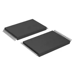
이미지는 참조용만
ADA4940-2ACPZ-R7
IC OPAMP DIFF 2 CIRCUIT 24LFCSP
- 제조업체
- Mfr.부분 #ADA4940-2ACPZ-R7
- 패키지 WFQFN-24
- 데이터시트
- 재고 있음7468
100% 원래 &새로운
배송 준비 24 시간
365 일 보장
RFQ 및더 많은 할인
사양
| Package | Tape & Reel (TR),Cut Tape (CT) |
| ProductStatus | Active |
| Type | ADC Driver |
| Applications | Driver |
| MountingType | Surface Mount |
| Package/Case | 24-WFQFN Exposed Pad, CSP |
개요
Description
The ADA4940-2 incorporates a high output drive capability, enabling it to drive heavy loads while maintaining linearity and low distortion. Its low total harmonic distortion (THD) and high common-mode rejection ratio (CMRR) ensure accurate signal amplification, making it an excellent choice for sensor interfacing and data acquisition systems.
The device is packaged in a small, thermally-efficient LFCSP (Lead Frame Chip Scale Package), facilitating easy integration into compact designs. Overall, the ADA4940-2 is ideal for applications requiring precision amplification with low noise and high linearity.
Features
1. Low Noise: Offers low input voltage noise (4.5 nV/√Hz), making it suitable for sensitive applications.
2. Wide Bandwidth: The amplifier has a unity-gain bandwidth of 65 MHz, allowing for high-speed signal processing.
3. High Slew Rate: Achieves a slew rate of 30 V/μs, facilitating fast signal transitions.
4. Low Distortion: Ensures low total harmonic distortion (THD), which is essential for high-fidelity applications.
5. Supply Voltage Range: Operates from ±2.5 V to ±15 V, providing flexibility for various power supply configurations.
6. Single and Dual Supply Operation: Supports both single and dual supply configurations.
7. Rail-to-Rail Output: Delivers output voltages that can swing close to the supply rails.
8. Temperature Range: Rated for operation from -40°C to +125°C, making it suitable for industrial applications.
These features position the ADA4940-2 as a robust choice for data acquisition, audio processing, and instrumentation applications.
Package
Pinout
Here is the pinout and their functions:
1. Pin 1: V- (Negative Supply Voltage)
2. Pin 2: R-Gain (External Resistor for Gain Adjustment)
3. Pin 3: IN+ (Positive Input)
4. Pin 4: IN- (Negative Input)
5. Pin 5: OUT (Output)
6. Pin 6: V+ (Positive Supply Voltage)
7. Pin 7: NC (No Connect)
8. Pin 8: NC (No Connect)
The device operates on a dual supply voltage and is designed for applications requiring high accuracy and low noise. It is commonly used in sensor signal conditioning, medical devices, and data acquisition systems.
Manufacturer
Application
Equivalent
배송
배송 방법We
DHL, FedEx, TNT, UPS 또는 선택한 다른 운송업체를 통해 글로벌 배송 서비스를 제공합니다.
배송 요금 참조 (DHL/FedEx):
DHL은: 배송 비용은 $25-$45 (0.5kg)에서 2-5 영업일의 추정적 배달 시간이 있습니다.
FedEx는: 배송 비용은 $25-$40 (0.5kg)에서 3-7 영업일의 추정적 배달 시간을 가지고 있습니다.
UPS는: 배송 비용은 $25-$45 (0.5kg)에서 3-7 영업일의 추정적 배달 시간을 가지고 있습니다.
TNT는: 배송 비용은 $25-$65 (0.5kg)에서 3-7 영업일의 추정적 배달 시간을 가지고 있습니다.
EMS는: 배송 비용은 $30-$50 (0.5kg)에서 7-15 영업일의 추정적 배달 시간을 제공합니다.
등록된 항공우편: 배송 비용은 $2-$4 (0.1kg), 예상 배달 시간 5-20 영업일.
지불
Payment Methods
지불 기간은 100% 사전 지불입니다.
현재, 우리는 아래 지불 방법만 받아들입니다.:
1. PayPal
2. 신용/직불 카드
3. 전선 전송
비슷한
-
![MX25R8035FM1IL0]() MX25R8035FM1IL0
Macronix
-
![MX25V1635FZNI]() MX25V1635FZNI
Macronix
-
![MX25V5126FM1I]() MX25V5126FM1I
Macronix
-
![MX25V4035FZUI]() MX25V4035FZUI
Macronix
-
![MX25V16066M2I02]() MX25V16066M2I02
Macronix
-
![MX30LF2G28AD-TI]() MX30LF2G28AD-TI
Macronix
-
![MX25U51279GXDR00]() MX25U51279GXDR00
Macronix
-
![MX25U6435FM2I-10G]() MX25U6435FM2I-10G
Macronix
-
![MX25L12833FZ2I-10G]() MX25L12833FZ2I-10..
Macronix
-
![MX25U25645GXDI00]() MX25U25645GXDI00
Macronix
-
![MX25L12835FZ2I-10G]() MX25L12835FZ2I-10..
Macronix
-
![MX29F040CTI-70G]() MX29F040CTI-70G
Macronix