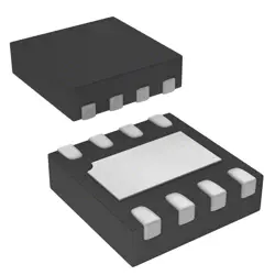
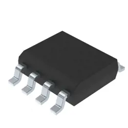
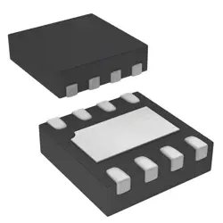
이미지는 참조용만
ADG5413FBCPZ
ADI +/--55V Fault Protected, +/-20V, +/-15V, +12V,
- 제조업체
- Mfr.부분 #ADG5413FBCPZ
- 패키지
- 데이터시트
- 재고 있음11982
100% 원래 &새로운
배송 준비 24 시간
365 일 보장
RFQ 및더 많은 할인
사양
| Packaging | Reel |
| Standard Pack Qty | 1500 |
개요
Description
Key specifications include a low on-resistance of approximately 0.8 ohms, high linearity, and fast switching speeds, ensuring efficient signal transfer with minimal signal degradation. The device operates over a supply voltage range of ±2.5V to ±15V, making it versatile for different circuit designs.
The ADG5413FBCPZ is constructed on a CMOS process, ensuring low power consumption and high reliability. It is available in a compact 16-lead TSSOP package, facilitating integration into space-constrained applications. The switch's logic control levels are compatible with TTL and CMOS, providing flexibility in digital interfacing.
Overall, the ADG5413FBCPZ is an excellent choice for applications requiring high-performance switching and routing of analog signals.
Features
1. Low On-Resistance: Typically 0.6 Ω at 5V, ensuring minimal signal distortion and power loss.
2. Wide Supply Voltage Range: Operates from 1.8V to 5.5V, suitable for a variety of applications.
3. Low Leakage Current: Ensures signal integrity with minimal leakage, typically 1 nA at 25°C.
4. Fast Switching Speed: Transition times of typically 15 ns (turn-on) and 15 ns (turn-off) for quick response.
5. High Bandwidth: Supports frequencies up to 1 GHz, making it suitable for RF applications.
6. Single Supply Operation: Allows for easier integration into designs with limited voltage supplies.
7. Small Package Size: Available in a compact LFCSP package, ideal for space-constrained applications.
8. Pin-Selectable Logic: Allows easy control of switch states via a simple logic interface.
These features make the ADG5413FBCPZ suitable for various applications, including video and RF signal switching, data acquisition systems, and audio signal routing.
Package
Pinout
The primary functions of the pins are as follows:
1. S1, S2 (Pins 1, 2): Signal inputs/outputs for switch A and B.
2. D1, D2 (Pins 3, 4): Drain connections for switch A and B.
3. GND (Pin 8): Ground connection.
4. COM (Pins 5, 6): Common pins for switch A and B.
5. VDD (Pin 7): Positive power supply.
6. IN1, IN2 (Pins 9, 10): Control inputs for switches A and B.
7. NC (Pins 11-16): No connect (not internally connected).
This device is used in applications requiring low distortion and low crosstalk, such as audio signal routing and data acquisition systems.
Manufacturer
Application
Equivalent
배송
배송 방법We
DHL, FedEx, TNT, UPS 또는 선택한 다른 운송업체를 통해 글로벌 배송 서비스를 제공합니다.
배송 요금 참조 (DHL/FedEx):
DHL은: 배송 비용은 $25-$45 (0.5kg)에서 2-5 영업일의 추정적 배달 시간이 있습니다.
FedEx는: 배송 비용은 $25-$40 (0.5kg)에서 3-7 영업일의 추정적 배달 시간을 가지고 있습니다.
UPS는: 배송 비용은 $25-$45 (0.5kg)에서 3-7 영업일의 추정적 배달 시간을 가지고 있습니다.
TNT는: 배송 비용은 $25-$65 (0.5kg)에서 3-7 영업일의 추정적 배달 시간을 가지고 있습니다.
EMS는: 배송 비용은 $30-$50 (0.5kg)에서 7-15 영업일의 추정적 배달 시간을 제공합니다.
등록된 항공우편: 배송 비용은 $2-$4 (0.1kg), 예상 배달 시간 5-20 영업일.
지불
Payment Methods
지불 기간은 100% 사전 지불입니다.
현재, 우리는 아래 지불 방법만 받아들입니다.:
1. PayPal
2. 신용/직불 카드
3. 전선 전송
비슷한
-
![MX25L3233FM1I-08Q]() MX25L3233FM1I-08Q
Macronix
-
![MX25V1635FZNI]() MX25V1635FZNI
Macronix
-
![MX29F400CBTI-70G]() MX29F400CBTI-70G
Macronix
-
![MX25V4035FZUI]() MX25V4035FZUI
Macronix
-
![MX25L8035EM2I-10G]() MX25L8035EM2I-10G
Macronix
-
![MX25U25643GZNI00]() MX25U25643GZNI00
Macronix
-
![MX25L2006EM1I-12G]() MX25L2006EM1I-12G
Macronix
-
![MX25R1635FZUIH0]() MX25R1635FZUIH0
Macronix
-
![MX25V1635FM2I]() MX25V1635FM2I
Macronix
-
![MX25U3232FZBI02]() MX25U3232FZBI02
Macronix
-
![MX25L12833FZ2I-10G]() MX25L12833FZ2I-10..
Macronix
-
![MX29LV160DTTI-70G]() MX29LV160DTTI-70G
Macronix