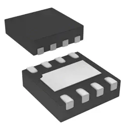
이미지는 참조용만
ADL5610ARKZ
ADI 2dB Noise Figure Gain Block
- 제조업체
- Mfr.부분 #ADL5610ARKZ
- 패키지
- 데이터시트
- 재고 있음5749
100% 원래 &새로운
배송 준비 24 시간
365 일 보장
RFQ 및더 많은 할인
사양
| Standard Pack Qty | 1000 |
개요
Description
Key features of the ADL5610ARKZ include a high gain of up to 20 dB, low noise figure, and excellent linearity, which contribute to improved signal integrity and overall system performance. The amplifier provides a programmable gain control (PGC) option, allowing for versatile operation across different signal conditions.
Its compact package and low power consumption make it ideal for integration into portable devices and systems. The ADL5610ARKZ is also noted for its thermal stability and reliability, ensuring consistent performance in diverse environmental conditions.
Overall, the ADL5610ARKZ is a vital component for engineers seeking to enhance the efficiency and effectiveness of RF signal amplification in modern communication technologies.
Features
1. Frequency Range: Operates from 0.1 GHz to 6.0 GHz, making it suitable for multiple RF bands.
2. Gain: Provides a high gain of up to 20 dB, ensuring strong amplification of weak signals.
3. High Linearity: Exhibits excellent linearity, enabling clean signal amplification and minimizing distortion.
4. Low Noise Figure: Features a low noise figure (NF), typically around 2.2 dB, enhancing signal-to-noise ratio (SNR).
5. Supply Voltage: Operates on a supply voltage range of 4.5 V to 5.5 V, allowing for flexibility in power supply designs.
6. Temperature Range: Designed to operate in a wide temperature range, from -40°C to +85°C, ensuring reliability in various environments.
7. Package Type: Offered in a compact, lead-free LFCSP package for minimized PCB space.
Overall, the ADL5610ARKZ is ideal for applications requiring robust performance in RF signal amplification.
Package
Pinout
The primary functions of the pins include:
1. Power Supply Pins: Provide operating voltage (VDD) to the amplifier.
2. Signal Input Pins: Accept RF input signals (RFIN1, RFIN2) for the two channels.
3. Signal Output Pins: Deliver amplified RF output signals (RFOUT1, RFOUT2).
4. Biasing Pins: Control the biasing of the amplifier for optimal performance.
5. Ground Pins: Provide a common ground reference (GND).
6. Control Pins: Enable or disable the amplifier functions, adjusting gain settings as needed.
For specific pin assignments and detailed electrical characteristics, refer to the ADL5610 datasheet.
Manufacturer
Application
Equivalent
배송
배송 방법We
DHL, FedEx, TNT, UPS 또는 선택한 다른 운송업체를 통해 글로벌 배송 서비스를 제공합니다.
배송 요금 참조 (DHL/FedEx):
DHL은: 배송 비용은 $25-$45 (0.5kg)에서 2-5 영업일의 추정적 배달 시간이 있습니다.
FedEx는: 배송 비용은 $25-$40 (0.5kg)에서 3-7 영업일의 추정적 배달 시간을 가지고 있습니다.
UPS는: 배송 비용은 $25-$45 (0.5kg)에서 3-7 영업일의 추정적 배달 시간을 가지고 있습니다.
TNT는: 배송 비용은 $25-$65 (0.5kg)에서 3-7 영업일의 추정적 배달 시간을 가지고 있습니다.
EMS는: 배송 비용은 $30-$50 (0.5kg)에서 7-15 영업일의 추정적 배달 시간을 제공합니다.
등록된 항공우편: 배송 비용은 $2-$4 (0.1kg), 예상 배달 시간 5-20 영업일.
지불
Payment Methods
지불 기간은 100% 사전 지불입니다.
현재, 우리는 아래 지불 방법만 받아들입니다.:
1. PayPal
2. 신용/직불 카드
3. 전선 전송
비슷한
-
![MX25R8035FM1IL0]() MX25R8035FM1IL0
Macronix
-
![MX25L3233FZBI-08Q]() MX25L3233FZBI-08Q
Macronix
-
![MX25L3233FM1I-08Q]() MX25L3233FM1I-08Q
Macronix
-
![MX25V1635FZNI]() MX25V1635FZNI
Macronix
-
![MX25V1635FZNQ03]() MX25V1635FZNQ03
Macronix
-
![MX25R3235FZNIL0]() MX25R3235FZNIL0
Macronix
-
![MX25L25673GMI-08G]() MX25L25673GMI-08G
Macronix
-
![MX25U51279GXDR00]() MX25U51279GXDR00
Macronix
-
![MX25U25643GZNI00]() MX25U25643GZNI00
Macronix
-
![MX25R1635FZUIH0]() MX25R1635FZUIH0
Macronix
-
![MX25V1635FM2I]() MX25V1635FM2I
Macronix
-
![MX25L12835FZ2I-10G]() MX25L12835FZ2I-10..
Macronix