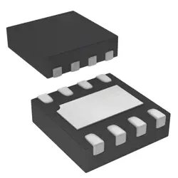
이미지는 참조용만
ADL5611ARKZ
ADI 2dB Noise Figure Gain Block
- 제조업체
- Mfr.부분 #ADL5611ARKZ
- 패키지
- 데이터시트
- 재고 있음21349
100% 원래 &새로운
배송 준비 24 시간
365 일 보장
RFQ 및더 많은 할인
사양
| Packaging | Reel |
| Standard Pack Qty | 1000 |
개요
Description
Key features include excellent linearity, low power consumption, and a compact package size. The amplifier supports a wide supply voltage range, allowing versatility in various applications. Its design incorporates matched input and output impedance, simplifying integration with other RF components.
The ADL5611ARKZ is ideal for enhancing signal integrity in applications like 5G, satellite communications, and other high-frequency systems. Additionally, its low thermal resistance ensures reliable operation over a range of conditions, making it a robust choice for engineers looking to optimize performance in their RF designs.
Features
1. Wide Frequency Range: Operates from 1 MHz to 3 GHz, making it suitable for various RF and microwave applications.
2. High Gain: Provides a gain of up to 20 dB, enhancing signal levels for improved performance.
3. Low Noise Figure: Offers a low noise figure, typically around 2.4 dB, which improves receiver sensitivity.
4. Single Supply Operation: Can operate on a single supply voltage, typically from 3.0 to 5.5 volts, simplifying design.
5. High Linearity: Exhibits excellent linearity, minimizing distortion and maintaining signal integrity.
6. Compact Package: Available in a compact 8-lead LFCSP package, facilitating integration into space-constrained designs.
7. Temperature Range: Rated for operation over a -40°C to +85°C temperature range, ensuring reliability in various environments.
These features make the ADL5611ARKZ suitable for applications in wireless infrastructure, instrumentation, and commercial systems.
Package
Pinout
The pin functions are as follows:
1. RF Input: Input for the RF signal.
2. GND: Ground connection.
3. RF Output: Output for the amplified RF signal.
4. VCC: Supply voltage input.
5. VBIAS: Bias voltage input.
6. RFIN: RF input (can be used for matching network).
7. RFB: Feedback pin for external components.
8. VOUT: Output voltage pin for testing.
9. NC (Not Connected): No connection; can be left floating or connected to ground.
10. GND (second instance): Additional ground pin for improved thermal and electrical performance.
11. GND (third instance): Another ground pin to minimize potential ground loop issues.
12. VCC (second instance): Additional supply voltage pin for improved power distribution.
Each pin plays a crucial role in the amplifier's operation, ensuring optimal performance across a range of RF applications.
Manufacturer
Application
Equivalent
배송
배송 방법We
DHL, FedEx, TNT, UPS 또는 선택한 다른 운송업체를 통해 글로벌 배송 서비스를 제공합니다.
배송 요금 참조 (DHL/FedEx):
DHL은: 배송 비용은 $25-$45 (0.5kg)에서 2-5 영업일의 추정적 배달 시간이 있습니다.
FedEx는: 배송 비용은 $25-$40 (0.5kg)에서 3-7 영업일의 추정적 배달 시간을 가지고 있습니다.
UPS는: 배송 비용은 $25-$45 (0.5kg)에서 3-7 영업일의 추정적 배달 시간을 가지고 있습니다.
TNT는: 배송 비용은 $25-$65 (0.5kg)에서 3-7 영업일의 추정적 배달 시간을 가지고 있습니다.
EMS는: 배송 비용은 $30-$50 (0.5kg)에서 7-15 영업일의 추정적 배달 시간을 제공합니다.
등록된 항공우편: 배송 비용은 $2-$4 (0.1kg), 예상 배달 시간 5-20 영업일.
지불
Payment Methods
지불 기간은 100% 사전 지불입니다.
현재, 우리는 아래 지불 방법만 받아들입니다.:
1. PayPal
2. 신용/직불 카드
3. 전선 전송
비슷한
-
![MX25R3235FZNIL0]() MX25R3235FZNIL0
Macronix
-
![MX25V16066M2I02]() MX25V16066M2I02
Macronix
-
![MX30LF2G28AD-TI]() MX30LF2G28AD-TI
Macronix
-
![MX25L25673GMI-08G]() MX25L25673GMI-08G
Macronix
-
![MX25U51279GXDR00]() MX25U51279GXDR00
Macronix
-
![MX25L2006EM1I-12G]() MX25L2006EM1I-12G
Macronix
-
![MX25U3232FZBI02]() MX25U3232FZBI02
Macronix
-
![MX25L12833FM2I-10G]() MX25L12833FM2I-10..
Macronix
-
![MX25L12833FZ2I-10G]() MX25L12833FZ2I-10..
Macronix
-
![MX25U25645GXDI00]() MX25U25645GXDI00
Macronix
-
![MX25L12835FZ2I-10G]() MX25L12835FZ2I-10..
Macronix
-
![MX29LV160DTTI-70G]() MX29LV160DTTI-70G
Macronix