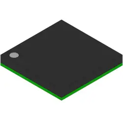
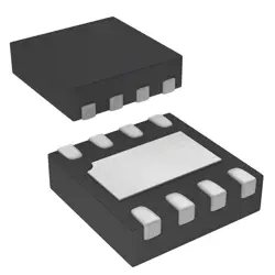
이미지는 참조용만
ADP7182ACPZN
ADI 200mA Negative Vout LDO
- 제조업체
- Mfr.부분 #ADP7182ACPZN
- 패키지
- 데이터시트
- 재고 있음17333
100% 원래 &새로운
배송 준비 24 시간
365 일 보장
RFQ 및더 많은 할인
사양
| Packaging | Reel |
| Standard Pack Qty | 3000 |
개요
Description
Key features include low output noise, high power supply rejection ratio (PSRR), and a wide input voltage range of 2.5 V to 20 V. The ADP7182 also includes built-in thermal overload protection, current limiting, and soft-start functionality, enhancing reliability and performance.
The device is packaged in a compact LFCSP (Lead Frame Chip Scale Package), which aids in thermal management and PCB space efficiency. It is ideal for applications such as RF and wireless systems, data converters, and imaging systems, where precision and stability are crucial. Overall, the ADP7182ACPZN is a robust choice for designers seeking high-performance voltage regulation in demanding environments.
Features
1. Output Voltage Range: Adjustable output voltage from 1.2V to 5.0V.
2. Low Dropout Voltage: Typically 200 mV at full load, ensuring efficient operation.
3. High Output Current: Supports up to 1.1 A output current, suitable for a variety of loads.
4. Power Supply Rejection Ratio (PSRR): Excellent PSRR performance, which enhances stability and reduces noise.
5. Thermal Protection: Integrated thermal shutdown to protect against overheating.
6. Short-Circuit Protection: Ensures safe operation under fault conditions.
7. Fast Transient Response: Maintains stability during load transients.
8. Low Quiescent Current: Minimizes power consumption, ideal for battery-operated devices.
9. Small Package: Available in a compact LFCSP package for space-constrained designs.
These features make the ADP7182ACPZN suitable for applications in portable electronics, communication devices, and high-performance analog circuits.
Package
Pinout
1. VIN (Pin 1): Input supply voltage.
2. GND (Pin 2): Ground reference.
3. VOUT (Pin 3): Regulated output voltage.
4. EN (Pin 4): Enable pin for turning the regulator on/off; active high.
5. NC (Pin 5): No connection; typically left floating.
6. VSET (Pin 6): Voltage setting pin used for adjusting the output voltage.
7. COMP (Pin 7): Compensation pin for stability; connects to an external capacitor and resistor.
8. PGND (Pin 8): Power ground; used for high current return paths.
This device provides excellent transient response and power supply rejection, making it suitable for powering sensitive analog circuits.
Manufacturer
Application
Equivalent
배송
배송 방법We
DHL, FedEx, TNT, UPS 또는 선택한 다른 운송업체를 통해 글로벌 배송 서비스를 제공합니다.
배송 요금 참조 (DHL/FedEx):
DHL은: 배송 비용은 $25-$45 (0.5kg)에서 2-5 영업일의 추정적 배달 시간이 있습니다.
FedEx는: 배송 비용은 $25-$40 (0.5kg)에서 3-7 영업일의 추정적 배달 시간을 가지고 있습니다.
UPS는: 배송 비용은 $25-$45 (0.5kg)에서 3-7 영업일의 추정적 배달 시간을 가지고 있습니다.
TNT는: 배송 비용은 $25-$65 (0.5kg)에서 3-7 영업일의 추정적 배달 시간을 가지고 있습니다.
EMS는: 배송 비용은 $30-$50 (0.5kg)에서 7-15 영업일의 추정적 배달 시간을 제공합니다.
등록된 항공우편: 배송 비용은 $2-$4 (0.1kg), 예상 배달 시간 5-20 영업일.
지불
Payment Methods
지불 기간은 100% 사전 지불입니다.
현재, 우리는 아래 지불 방법만 받아들입니다.:
1. PayPal
2. 신용/직불 카드
3. 전선 전송
비슷한
-
![MX25L3233FZBI-08Q]() MX25L3233FZBI-08Q
Macronix
-
![MX25L3233FM1I-08Q]() MX25L3233FM1I-08Q
Macronix
-
![MX25V1635FZNI]() MX25V1635FZNI
Macronix
-
![MX25V1635FZNQ03]() MX25V1635FZNQ03
Macronix
-
![MX25R3235FZNIL0]() MX25R3235FZNIL0
Macronix
-
![MX25V16066M2I02]() MX25V16066M2I02
Macronix
-
![MX25L8035EM2I-10G]() MX25L8035EM2I-10G
Macronix
-
![MX29GL512FHXFI-11G]() MX29GL512FHXFI-11..
Macronix
-
![MX25U3232FZBI02]() MX25U3232FZBI02
Macronix
-
![MX25U6435FM2I-10G]() MX25U6435FM2I-10G
Macronix
-
![MX25L12833FZ2I-10G]() MX25L12833FZ2I-10..
Macronix
-
![MX25L25645GXDI-08G]() MX25L25645GXDI-08..
Macronix