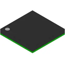
이미지는 참조용만
ADP7183ACPZN
ADI Ultra Low Noise, High PSR
- 제조업체
- Mfr.부분 #ADP7183ACPZN
- 패키지
- 데이터시트
- 재고 있음6677
100% 원래 &새로운
배송 준비 24 시간
365 일 보장
RFQ 및더 많은 할인
사양
| Standard Pack Qty | 3000 |
개요
Description
Key features include low dropout voltage (typically around 200 mV), high output current capability (up to 1A), and excellent transient response. The ADP7183 also incorporates thermal shutdown and current limit protection, ensuring safe operation under various conditions. Additionally, it has a low quiescent current, making it ideal for battery-powered applications.
The package type is compact, which aids in space-constrained designs. The ADP7183 is commonly used in audio equipment, RF applications, and portable devices where power efficiency and low noise are critical. Overall, it is a robust choice for designers seeking reliable voltage regulation solutions.
Features
1. Output Voltage Range: Adjustable output voltage from 1.2V to 3.6V.
2. Low Dropout Voltage: Typically 200 mV at 1 A load, allowing for efficient operation with minimal input-output voltage difference.
3. High Output Current: Capable of sourcing up to 1 A of output current.
4. Low Quiescent Current: Offers low quiescent current, enhancing battery life in portable applications.
5. Power Good Indicator: Integrated power good signal to indicate proper output voltage levels.
6. Thermal Protection: Built-in thermal shutdown feature to prevent overheating.
7. Package Options: Available in compact packages like LFCSP and SOIC, suitable for space-constrained designs.
8. Wide Operating Temperature Range: Operates from -40°C to +125°C, ensuring reliability in various environments.
These features make the ADP7183ACPZN ideal for use in powering sensitive analog circuits, RF applications, and battery-powered devices.
Package
Pinout
1. VIN: Input voltage.
2. GND: Ground reference.
3. VOUT: Regulated output voltage.
4. EN: Enable pin for activating/deactivating the regulator.
5. PG: Power good output; indicates if the output is within the specified range.
6. BYPASS: Bypass capacitor pin to improve transient response.
7. NC: No connect; not internally connected.
8. ADJ: Adjustment pin for setting the output voltage (if adjustable version).
This component is typically used in applications requiring stable output voltages with high power supply rejection ratios and low noise.
Manufacturer
Application
Equivalent
1. MIC5205 - Microchip Technology
2. TPS7A33 - Texas Instruments
3. LT1085 - Analog Devices
4. LM1117 - Texas Instruments
5. NCP1117 - ON Semiconductor
Always verify specifications like output voltage, current, and dropout voltage for compatibility.
배송
배송 방법We
DHL, FedEx, TNT, UPS 또는 선택한 다른 운송업체를 통해 글로벌 배송 서비스를 제공합니다.
배송 요금 참조 (DHL/FedEx):
DHL은: 배송 비용은 $25-$45 (0.5kg)에서 2-5 영업일의 추정적 배달 시간이 있습니다.
FedEx는: 배송 비용은 $25-$40 (0.5kg)에서 3-7 영업일의 추정적 배달 시간을 가지고 있습니다.
UPS는: 배송 비용은 $25-$45 (0.5kg)에서 3-7 영업일의 추정적 배달 시간을 가지고 있습니다.
TNT는: 배송 비용은 $25-$65 (0.5kg)에서 3-7 영업일의 추정적 배달 시간을 가지고 있습니다.
EMS는: 배송 비용은 $30-$50 (0.5kg)에서 7-15 영업일의 추정적 배달 시간을 제공합니다.
등록된 항공우편: 배송 비용은 $2-$4 (0.1kg), 예상 배달 시간 5-20 영업일.
지불
Payment Methods
지불 기간은 100% 사전 지불입니다.
현재, 우리는 아래 지불 방법만 받아들입니다.:
1. PayPal
2. 신용/직불 카드
3. 전선 전송
비슷한
-
![MX25R8035FM1IL0]() MX25R8035FM1IL0
Macronix
-
![MX25V2033FM1I]() MX25V2033FM1I
Macronix
-
![MX30LF2G28AD-TI]() MX30LF2G28AD-TI
Macronix
-
![MX25L8035EM2I-10G]() MX25L8035EM2I-10G
Macronix
-
![MX25L25673GMI-10G]() MX25L25673GMI-10G
Macronix
-
![MX29GL512FHXFI-11G]() MX29GL512FHXFI-11..
Macronix
-
![MX25U51279GXDR00]() MX25U51279GXDR00
Macronix
-
![MX25R1635FZUIH0]() MX25R1635FZUIH0
Macronix
-
![MX25L12833FZ2I-10G]() MX25L12833FZ2I-10..
Macronix
-
![MX25U25645GXDI00]() MX25U25645GXDI00
Macronix
-
![MX29LV160DTTI-70G]() MX29LV160DTTI-70G
Macronix
-
![MX29F800CBTI-70G]() MX29F800CBTI-70G
Macronix