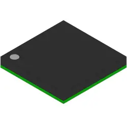
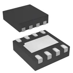
이미지는 참조용만
AM29F040B-70EF
NOR Flash 4M (512Kx8) 70ns 5v Parallel NOR Flash
- 제조업체
- Mfr.부분 #AM29F040B-70EF
- 패키지
- 데이터시트 AM29F040B-70EF DataSheet
- 재고 있음4873
100% 원래 &새로운
배송 준비 24 시간
365 일 보장
RFQ 및더 많은 할인
사양
| Packaging | Tray |
| Standard Pack Qty | 156 |
개요
Description
Key features include:
1. Single 5V Supply: Simplifies circuit design.
2. Multiple Programming Modes: Supports sector-based programming and erasing, enhancing flexibility.
3. Endurance: Capable of withstanding up to 100,000 program/erase cycles, making it suitable for applications with frequent updates.
4. Data Retention: Offers a data retention period of at least 20 years under typical conditions.
5. Parallel I/O: Facilitates easy integration with microcontrollers and other digital systems.
The AM29F040B-70EF is popular for its reliability, performance, and ease of use in various electronic applications.
Features
1. Architecture: It utilizes a single 5V supply and offers a NAND-type Flash memory architecture.
2. Access Time: The device has a maximum access time of 70 ns, enabling fast read operations.
3. Data I/O: It supports an 8-bit data bus, allowing for efficient data transfers.
4. Sector Erase: The memory is organized into 16 sectors of 32 Kbytes each, allowing for flexible erase capabilities.
5. Program and Erase Cycles: It supports up to 10,000 program/erase cycles, ensuring reliability over time.
6. Data Retention: The typical data retention period is about 20 years, suitable for long-term storage.
7. Compatibility: It is compatible with existing EPROM and EEPROM design protocols, facilitating easier integration into systems.
These features make the AM29F040B-70EF a reliable choice for applications requiring non-volatile storage, such as embedded systems and consumer electronics.
Package
Pinout
Pin Count: 32 pins
Key Functions:
1. Address Inputs (A0 - A19): Used to select addresses for reading or programming data stored in the memory.
2. Data Inputs/Outputs (D0 - D7): 8-bit wide data bus for reading from and writing to the memory.
3. Chip Enable (CE): Activates the chip for read or write operations.
4. Output Enable (OE): Enables data output during read operations.
5. Write Enable (WE): Activates write operations.
6. Reset (RESET): Resets the memory to its initial state.
7. Vcc: Power supply pin.
8. GND: Ground connection.
This device is commonly used in applications requiring non-volatile memory storage, such as firmware storage in embedded systems.
Manufacturer
Application
Equivalent
1. Intel 28F040
2. Micron MT28F040
3. Winbond W29EE040
4. STMicroelectronics M29F040
5. SST39LF040
Ensure to check specific datasheets for pin compatibility and electrical characteristics when considering substitutes.
배송
배송 방법We
DHL, FedEx, TNT, UPS 또는 선택한 다른 운송업체를 통해 글로벌 배송 서비스를 제공합니다.
배송 요금 참조 (DHL/FedEx):
DHL은: 배송 비용은 $25-$45 (0.5kg)에서 2-5 영업일의 추정적 배달 시간이 있습니다.
FedEx는: 배송 비용은 $25-$40 (0.5kg)에서 3-7 영업일의 추정적 배달 시간을 가지고 있습니다.
UPS는: 배송 비용은 $25-$45 (0.5kg)에서 3-7 영업일의 추정적 배달 시간을 가지고 있습니다.
TNT는: 배송 비용은 $25-$65 (0.5kg)에서 3-7 영업일의 추정적 배달 시간을 가지고 있습니다.
EMS는: 배송 비용은 $30-$50 (0.5kg)에서 7-15 영업일의 추정적 배달 시간을 제공합니다.
등록된 항공우편: 배송 비용은 $2-$4 (0.1kg), 예상 배달 시간 5-20 영업일.
지불
Payment Methods
지불 기간은 100% 사전 지불입니다.
현재, 우리는 아래 지불 방법만 받아들입니다.:
1. PayPal
2. 신용/직불 카드
3. 전선 전송
비슷한
-
![MX25L3233FM1I-08Q]() MX25L3233FM1I-08Q
Macronix
-
![MX25V5126FM1I]() MX25V5126FM1I
Macronix
-
![MX25V16066M1I02]() MX25V16066M1I02
Macronix
-
![MX25V16066M2I02]() MX25V16066M2I02
Macronix
-
![MX25L8035EM2I-10G]() MX25L8035EM2I-10G
Macronix
-
![MX25R6435FBDIL0]() MX25R6435FBDIL0
Macronix
-
![MX25L25673GMI-08G]() MX25L25673GMI-08G
Macronix
-
![MX29GL512FHXFI-11G]() MX29GL512FHXFI-11..
Macronix
-
![MX25U51279GXDR00]() MX25U51279GXDR00
Macronix
-
![MX25U3232FZBI02]() MX25U3232FZBI02
Macronix
-
![MX25L6433FM2I-08G]() MX25L6433FM2I-08G
Macronix
-
![MX25L12833FZ2I-10G]() MX25L12833FZ2I-10..
Macronix