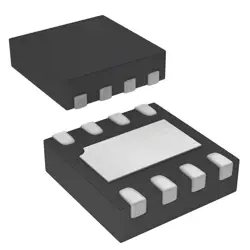
이미지는 참조용만
CD4016BM96
IC BILATERAL SW 1 X 1:1 14SOIC
- 제조업체
- Mfr.부분 #CD4016BM96
- 패키지 SOIC (D)-14
- 데이터시트
- 재고 있음3733
100% 원래 &새로운
배송 준비 24 시간
365 일 보장
RFQ 및더 많은 할인
사양
| Package | Tape & Reel (TR),Cut Tape (CT) |
| Series | 4000B |
| ProductStatus | Active |
| Type | Bilateral, FET Switches |
| Circuit | 1 x 1:1 |
| IndependentCircuits | 4 |
| VoltageSupplySource | Dual Supply |
| Voltage-Supply | 3V ~ 18V |
| OperatingTemperature | -55°C ~ 125°C |
| MountingType | Surface Mount |
| Package/Case | 14-SOIC (0.154, 3.90mm Width) |
개요
Description
Designed for low power consumption, the CD4016BM96 operates over a wide voltage range, typically between 3V and 15V, making it suitable for battery-operated devices and other low-voltage applications. The IC is characterized by low ON resistance, enabling efficient signal transmission with minimal distortion.
Common applications include analog signal processing, data multiplexing, and signal isolation. Its ability to handle both analog and digital signals makes it a flexible choice for designers in telecommunications, audio equipment, and sensor interfacing. The CD4016BM96 is available in various package types, including DIP and SOIC, facilitating integration into different circuit designs.
Features
1. Quad Switch Configuration: Contains four independent switches that can be used to control analog signals.
2. Low On-Resistance: Provides a low on-resistance (typically 10 Ω at V_DD = 5V), ensuring minimal signal distortion.
3. Wide Supply Voltage Range: Operates from a supply voltage of 3V to 15V, making it versatile for various applications.
4. High Speed: Capable of switching speeds suitable for audio and data applications.
5. Low Power Consumption: Consumes low quiescent current, enhancing battery-operated device performance.
6. TTL Compatible: Can be directly interfaced with TTL logic levels, simplifying circuit design.
7. Bidirectional Signal Flow: Allows signals to pass in either direction, offering flexibility in circuit configurations.
Applications include audio signal routing, data switching, and general-purpose signal manipulation in digital and analog electronics.
Package
Pinout
Pin Functionality:
1. Pin 1-4: Switch 1 (S1), Switch 2 (S2), Switch 3 (S3), Switch 4 (S4) – These pins connect to the signal.
2. Pin 5-8: Control pins (C1, C2, C3, C4) – These pins control the gates of the switches, enabling or disabling the respective switch.
3. Pin 9: Ground (VSS) – This pin is connected to the ground.
4. Pin 10-13: Additional switch pins (input/output for the switches).
5. Pin 14: Power supply (VDD) – This pin connects to the positive supply voltage.
The CD4016BM96 allows for low on-resistance switching, making it suitable for various applications in analog signal processing.
Manufacturer
Application
Equivalent
배송
배송 방법We
DHL, FedEx, TNT, UPS 또는 선택한 다른 운송업체를 통해 글로벌 배송 서비스를 제공합니다.
배송 요금 참조 (DHL/FedEx):
DHL은: 배송 비용은 $25-$45 (0.5kg)에서 2-5 영업일의 추정적 배달 시간이 있습니다.
FedEx는: 배송 비용은 $25-$40 (0.5kg)에서 3-7 영업일의 추정적 배달 시간을 가지고 있습니다.
UPS는: 배송 비용은 $25-$45 (0.5kg)에서 3-7 영업일의 추정적 배달 시간을 가지고 있습니다.
TNT는: 배송 비용은 $25-$65 (0.5kg)에서 3-7 영업일의 추정적 배달 시간을 가지고 있습니다.
EMS는: 배송 비용은 $30-$50 (0.5kg)에서 7-15 영업일의 추정적 배달 시간을 제공합니다.
등록된 항공우편: 배송 비용은 $2-$4 (0.1kg), 예상 배달 시간 5-20 영업일.
지불
Payment Methods
지불 기간은 100% 사전 지불입니다.
현재, 우리는 아래 지불 방법만 받아들입니다.:
1. PayPal
2. 신용/직불 카드
3. 전선 전송
비슷한
-
![MX25L3233FZBI-08Q]() MX25L3233FZBI-08Q
Macronix
-
![MX25L3233FM1I-08Q]() MX25L3233FM1I-08Q
Macronix
-
![MX25V1635FZNI]() MX25V1635FZNI
Macronix
-
![MX25V1635FZNQ03]() MX25V1635FZNQ03
Macronix
-
![MX25V5126FM1I]() MX25V5126FM1I
Macronix
-
![MX25V4035FZUI]() MX25V4035FZUI
Macronix
-
![MX25V2033FM1I]() MX25V2033FM1I
Macronix
-
![MX25U3232FZBI02]() MX25U3232FZBI02
Macronix
-
![MX25L12833FM2I-10G]() MX25L12833FM2I-10..
Macronix
-
![MX25L12833FZ2I-10G]() MX25L12833FZ2I-10..
Macronix
-
![MX25U25645GXDI00]() MX25U25645GXDI00
Macronix
-
![MX29F800CBTI-70G]() MX29F800CBTI-70G
Macronix