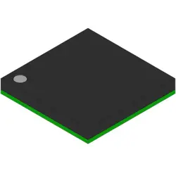
이미지는 참조용만
CDCE62002RHBR
IC CLOCK GENERATOR 32VQFN
- 제조업체
- Mfr.부분 #CDCE62002RHBR
- 패키지
- 데이터시트
- 재고 있음4586
100% 원래 &새로운
배송 준비 24 시간
365 일 보장
RFQ 및더 많은 할인
사양
| Part Status | Active |
| DigiKey Programmable | Not Verified |
| Type | Clock Generator |
| PLL | Yes |
| Input | LVCMOS, LVDS, LVPECL, Crystal |
| Output | LVCMOS, LVDS, LVPECL |
| Number of Circuits | 1 |
| Ratio - Input:Output | 2:2 |
| Differential - Input:Output | Yes/Yes |
| Frequency - Max | 1.175GHz |
| Divider/Multiplier | Yes/No |
| Voltage - Supply | 3V ~ 3.6V |
| Operating Temperature | -40°C ~ 85°C |
| Mounting Type | Surface Mount |
| Package / Case | 32-VFQFN Exposed Pad |
| Supplier Device Package | 32-VQFN (5x5) |
| Base Product Number | CDCE62002 |
개요
Description
Key characteristics include the ability to program output frequencies, support for differential and single-ended outputs, and various output formats. Additionally, it offers integrated power management features, allowing for efficient operation and reducing power consumption. The CDCE62002RHBR is designed for easy integration into systems, with an I2C interface for configuration and control.
Overall, this component is essential for applications requiring high-frequency precision and flexibility in clock management.
Features
1. Low Jitter Performance: Ensures high signal integrity with minimal phase noise.
2. Multiple Outputs: Offers multiple buffered clock outputs, typically up to 2.
3. Wide Frequency Range: Capable of handling a broad frequency range, which allows it to support various clock sources.
4. Input Compatibility: Accepts a variety of input signal types, providing flexibility in system design.
5. Power Supply Options: Operates on low voltage (typically 3.3V), promoting energy efficiency.
6. Applications: Ideal for use in high-speed communication systems, such as Ethernet and PCIe.
7. Thermal and Electrical Performance: Designed for minimal heat generation and reliable operation under various conditions.
This device is suitable for applications where precise clock management is crucial.
Package
Pinout
Pin Functions:
1. Power and Ground Pins:
- VDD: Supply voltage
- GND: Ground
2. Input Pins:
- XTAL1, XTAL2: Crystal oscillator connections for specifying the reference frequency.
- REFCLK: External reference clock input.
3. Output Pins:
- CLKOUT0 - CLKOUT5: Multiple clock output signals with programmable frequency and duty cycle.
4. Configuration Pins:
- I2C: SDA, SCL pins for serial data communication for configuration.
- /RESET: Active low reset pin.
- /S0, /S1: Select pins for mode selection.
5. Status Pins:
- LOCK: Indicates the lock status of the PLL.
This device is designed for applications requiring precise clock generation with reduced jitter and flexibility in frequency settings.
Manufacturer
Application
Equivalent
배송
배송 방법We
DHL, FedEx, TNT, UPS 또는 선택한 다른 운송업체를 통해 글로벌 배송 서비스를 제공합니다.
배송 요금 참조 (DHL/FedEx):
DHL은: 배송 비용은 $25-$45 (0.5kg)에서 2-5 영업일의 추정적 배달 시간이 있습니다.
FedEx는: 배송 비용은 $25-$40 (0.5kg)에서 3-7 영업일의 추정적 배달 시간을 가지고 있습니다.
UPS는: 배송 비용은 $25-$45 (0.5kg)에서 3-7 영업일의 추정적 배달 시간을 가지고 있습니다.
TNT는: 배송 비용은 $25-$65 (0.5kg)에서 3-7 영업일의 추정적 배달 시간을 가지고 있습니다.
EMS는: 배송 비용은 $30-$50 (0.5kg)에서 7-15 영업일의 추정적 배달 시간을 제공합니다.
등록된 항공우편: 배송 비용은 $2-$4 (0.1kg), 예상 배달 시간 5-20 영업일.
지불
Payment Methods
지불 기간은 100% 사전 지불입니다.
현재, 우리는 아래 지불 방법만 받아들입니다.:
1. PayPal
2. 신용/직불 카드
3. 전선 전송
비슷한
-
![MX25R8035FM1IL0]() MX25R8035FM1IL0
Macronix
-
![MX25L3233FM1I-08Q]() MX25L3233FM1I-08Q
Macronix
-
![MX25V1635FZNI]() MX25V1635FZNI
Macronix
-
![MX29F400CBTI-70G]() MX29F400CBTI-70G
Macronix
-
![MX25V5126FM1I]() MX25V5126FM1I
Macronix
-
![MX25V2033FM1I]() MX25V2033FM1I
Macronix
-
![MX25R6435FBDIL0]() MX25R6435FBDIL0
Macronix
-
![MX29GL512FHXFI-11G]() MX29GL512FHXFI-11..
Macronix
-
![MX25L2006EM1I-12G]() MX25L2006EM1I-12G
Macronix
-
![MX25R1635FZUIH0]() MX25R1635FZUIH0
Macronix
-
![MX25V1635FM2I]() MX25V1635FM2I
Macronix
-
![MX25L6433FM2I-08G]() MX25L6433FM2I-08G
Macronix