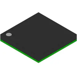
이미지는 참조용만
EP1K50FC256-2N
IC FPGA 186 I/O 256FBGA
- 제조업체
- Mfr.부분 #EP1K50FC256-2N
- 패키지
- 데이터시트
- 재고 있음2753
100% 원래 &새로운
배송 준비 24 시간
365 일 보장
RFQ 및더 많은 할인
사양
| Series | ACEX-1K® |
| Part Status | Obsolete |
| DigiKey Programmable | Not Verified |
| Total RAM Bits | 40960 |
| Number of I/O | 186 |
| Number of Gates | 199000 |
| Voltage - Supply | 2.375V ~ 2.625V |
| Mounting Type | Surface Mount |
| Operating Temperature | 0°C ~ 70°C (TA) |
| Package / Case | 256-BGA |
| Supplier Device Package | 256-FBGA (17x17) |
| Base Product Number | EP1K50 |
| Number of Logic Elements/Cells | 2880 |
| Number of LABs/CLBs | 360 |
개요
Description
The FPGA is housed in a 256-pin Fine Pitch Ball Grid Array (FBGA) package, facilitating easy integration into various electronic designs. Its architecture supports a range of digital signal processing applications, including communications, automotive, and industrial control.
The EP1K50FC256-2N operates at a maximum clock frequency of 200 MHz, providing robust processing capability. Additionally, it supports various I/O standards, enabling compatibility with different interfacing requirements. The FPGA can be programmed using hardware description languages such as VHDL or Verilog, allowing for custom logic designs tailored to specific application needs. Overall, it is an ideal choice for engineers seeking a versatile and economical solution for their digital design projects.
Features
1. Logic Elements: Approximately 50,000 logic elements provide a flexible architecture for customizable designs.
2. Embedded Memory: Up to 2.5 Mbits of embedded memory blocks for efficient data storage.
3. I/O Pins: 256 pins, configurable for various I/O standards to interface with external devices.
4. DSP Blocks: Includes dedicated DSP (Digital Signal Processing) blocks for high-performance arithmetic operations.
5. Power Efficiency: Designed for low power consumption, making it suitable for portable applications.
6. Configuration: Supports various configuration modes, including JTAG and passive serial.
7. Development Support: Compatible with Altera’s Quartus Prime software for design and simulation.
This device is ideal for applications requiring moderate complexity, such as digital signal processing, automotive systems, and communication devices.
Package
Pinout
The device is designed for a range of applications and includes various functionalities such as:
- Logic elements for implementing custom digital circuits.
- I/O pins that support various I/O standards for interfacing with external components.
- Memory blocks for on-chip data storage.
- DSP blocks for digital signal processing tasks.
This FPGA is optimized for low power and cost-effective solutions, making it suitable for consumer electronics, automotive applications, and other embedded systems.
Manufacturer
Application
Equivalent
1. Xilinx Spartan-6 (e.g., XC6SLX50)
2. Lattice MachXO2 (e.g., LCXO2-1200)
3. Microsemi SmartFusion (e.g., M2S010)
Note that while these alternatives may offer similar capabilities, they may differ in architecture, features, and specific use cases. Always check datasheets for compatibility.
배송
배송 방법We
DHL, FedEx, TNT, UPS 또는 선택한 다른 운송업체를 통해 글로벌 배송 서비스를 제공합니다.
배송 요금 참조 (DHL/FedEx):
DHL은: 배송 비용은 $25-$45 (0.5kg)에서 2-5 영업일의 추정적 배달 시간이 있습니다.
FedEx는: 배송 비용은 $25-$40 (0.5kg)에서 3-7 영업일의 추정적 배달 시간을 가지고 있습니다.
UPS는: 배송 비용은 $25-$45 (0.5kg)에서 3-7 영업일의 추정적 배달 시간을 가지고 있습니다.
TNT는: 배송 비용은 $25-$65 (0.5kg)에서 3-7 영업일의 추정적 배달 시간을 가지고 있습니다.
EMS는: 배송 비용은 $30-$50 (0.5kg)에서 7-15 영업일의 추정적 배달 시간을 제공합니다.
등록된 항공우편: 배송 비용은 $2-$4 (0.1kg), 예상 배달 시간 5-20 영업일.
지불
Payment Methods
지불 기간은 100% 사전 지불입니다.
현재, 우리는 아래 지불 방법만 받아들입니다.:
1. PayPal
2. 신용/직불 카드
3. 전선 전송
비슷한
-
![MX25L3233FZBI-08Q]() MX25L3233FZBI-08Q
Macronix
-
![MX25V1635FZNI]() MX25V1635FZNI
Macronix
-
![MX29F400CBTI-70G]() MX29F400CBTI-70G
Macronix
-
![MX25R3235FZNIL0]() MX25R3235FZNIL0
Macronix
-
![MX25L8035EM2I-10G]() MX25L8035EM2I-10G
Macronix
-
![MX29GL512FHXFI-11G]() MX29GL512FHXFI-11..
Macronix
-
![MX25V1635FM2I]() MX25V1635FM2I
Macronix
-
![MX25U6435FM2I-10G]() MX25U6435FM2I-10G
Macronix
-
![MX25L12833FZNI-10G]() MX25L12833FZNI-10..
Macronix
-
![MX29F040CTI-70G]() MX29F040CTI-70G
Macronix
-
![MX29F800CBTI-70G]() MX29F800CBTI-70G
Macronix
-
![MX29LV640ETTI-70G]() MX29LV640ETTI-70G
Macronix