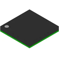
이미지는 참조용만
EP3C55F484I7N
IC FPGA 327 I/O 484FBGA
- 제조업체
- Mfr.부분 #EP3C55F484I7N
- 패키지 FBGA-484
- 데이터시트
- 재고 있음5001
100% 원래 &새로운
배송 준비 24 시간
365 일 보장
RFQ 및더 많은 할인
사양
| Package | Tray |
| Series | Cyclone® III |
| ProductStatus | Active |
| NumberofLABs/CLBs | 3491 |
| NumberofLogicElements/Cells | 55856 |
| TotalRAMBits | 2396160 |
| NumberofI/O | 327 |
| Voltage-Supply | 1.15V ~ 1.25V |
| MountingType | Surface Mount |
| OperatingTemperature | -40°C ~ 100°C (TJ) |
| Package/Case | 484-BGA |
개요
Description
Key specifications include a maximum operating frequency of up to 150 MHz, multiple I/O standards, and integrated memory options. The 484-pin FinePitch Ball Grid Array (FBGA) package facilitates high-density applications, making it suitable for compact designs. The device operates at various voltage levels, enhancing compatibility with different systems.
Developers can leverage the Quartus Prime software for design entry, simulation, and timing analysis, making it easier to implement and validate complex algorithms. The EP3C55F484I7N is ideal for applications in telecommunications, automotive, and consumer electronics, where adaptability and performance are crucial.
Features
1. Logic Elements: It contains around 55,000 logic elements, enabling complex logic functions.
2. Memory: Offers up to 2 Mbits of embedded memory, supporting various applications requiring data storage.
3. I/O Pins: Provides up to 484 I/O pins, facilitating extensive connectivity options for peripherals and external devices.
4. High-Speed Interfaces: Supports standard interfaces such as SPI, I2C, and UART, along with high-speed transceivers for communication.
5. Power Efficiency: Operates at low power consumption levels, making it suitable for battery-powered and compact devices.
6. Design Flexibility: Compatible with Intel Quartus® Prime software for design and development, allowing users to implement custom logic easily.
7. Operating Voltage: Typically operates at 1.2V for core and 3.3V for I/O, enhancing device compatibility.
These features make the EP3C55F484I7N ideal for applications in automotive, telecommunications, and consumer electronics.
Package
Pinout
The pins serve various functions, including:
1. I/O Pins: Configurable for general-purpose input/output (GPIO), supporting various voltage standards.
2. Power Supply Pins: For powering the FPGA, typically including VCC and ground (GND) connections.
3. Configuration Pins: Used for loading the configuration data into the FPGA upon startup.
4. Clock Pins: Dedicated pins for clock signals to drive the internal circuitry.
5. JTAG Pins: For in-system programming and debugging.
The FPGA is designed for applications in communications, automotive, and industrial fields, providing flexibility and performance in a compact package.
Manufacturer
Application
Equivalent
배송
배송 방법We
DHL, FedEx, TNT, UPS 또는 선택한 다른 운송업체를 통해 글로벌 배송 서비스를 제공합니다.
배송 요금 참조 (DHL/FedEx):
DHL은: 배송 비용은 $25-$45 (0.5kg)에서 2-5 영업일의 추정적 배달 시간이 있습니다.
FedEx는: 배송 비용은 $25-$40 (0.5kg)에서 3-7 영업일의 추정적 배달 시간을 가지고 있습니다.
UPS는: 배송 비용은 $25-$45 (0.5kg)에서 3-7 영업일의 추정적 배달 시간을 가지고 있습니다.
TNT는: 배송 비용은 $25-$65 (0.5kg)에서 3-7 영업일의 추정적 배달 시간을 가지고 있습니다.
EMS는: 배송 비용은 $30-$50 (0.5kg)에서 7-15 영업일의 추정적 배달 시간을 제공합니다.
등록된 항공우편: 배송 비용은 $2-$4 (0.1kg), 예상 배달 시간 5-20 영업일.
지불
Payment Methods
지불 기간은 100% 사전 지불입니다.
현재, 우리는 아래 지불 방법만 받아들입니다.:
1. PayPal
2. 신용/직불 카드
3. 전선 전송
비슷한
-
![MX25V1635FZNI]() MX25V1635FZNI
Macronix
-
![MX25V1635FZNQ03]() MX25V1635FZNQ03
Macronix
-
![MX29F400CBTI-70G]() MX29F400CBTI-70G
Macronix
-
![MX25V2033FM1I]() MX25V2033FM1I
Macronix
-
![MX25V16066M2I02]() MX25V16066M2I02
Macronix
-
![MX30LF2G28AD-TI]() MX30LF2G28AD-TI
Macronix
-
![MX25L25673GMI-08G]() MX25L25673GMI-08G
Macronix
-
![MX25L25673GMI-10G]() MX25L25673GMI-10G
Macronix
-
![MX29GL512FHXFI-11G]() MX29GL512FHXFI-11..
Macronix
-
![MX25U51279GXDR00]() MX25U51279GXDR00
Macronix
-
![MX25U25643GZNI00]() MX25U25643GZNI00
Macronix
-
![MX25R1635FZUIH0]() MX25R1635FZUIH0
Macronix