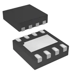
이미지는 참조용만
GD25LE32DLIGR
IC FLASH 32MBIT SPI/QUAD 21WLCSP
- 제조업체
- Mfr.부분 #GD25LE32DLIGR
- 패키지
- 데이터시트
- 재고 있음7762
100% 원래 &새로운
배송 준비 24 시간
365 일 보장
RFQ 및더 많은 할인
사양
| Part Status | Active |
| Base Product Number | GD25LE32 |
| DigiKey Programmable | Not Verified |
| Memory Type | Non-Volatile |
| Memory Format | FLASH |
| Technology | FLASH - NOR |
| Memory Size | 32Mbit |
| Memory Organization | 4M x 8 |
| Memory Interface | SPI - Quad I/O |
| Clock Frequency | 120 MHz |
| Write Cycle Time - Word, Page | 2.4ms |
| Voltage - Supply | 1.65V ~ 2V |
| Operating Temperature | -40°C ~ 85°C (TA) |
| Mounting Type | Surface Mount |
| Package | 21-XFBGA, WLSCP |
| Supplier Device Package | 21-WLCSP |
| Packaging | Tape & Reel (TR) |
개요
Description
Key features include:
- Memory Density: 32 Megabits (4 Megabytes).
- Operating Voltage: Typically operates at 3.3V, with a low-power mode to reduce energy consumption.
- Speed: Supports high-speed read operations, with speeds up to 104 MHz in dual and quad SPI modes.
- Data Transfer: Offers multiple data transfer modes, including single, dual, and quad I/O.
- Endurance and Reliability: Generally supports up to 100,000 program/erase cycles and has a data retention of over 20 years.
The GD25LE32DLIGR is commonly used in applications requiring reliable data storage, such as firmware storage and configuration settings in microcontrollers.
Features
Key features include:
- 32Mb (4MB) storage capacity
- Dual and quad SPI interface support
- High-speed data transfer rates
- 1.8V to 3.6V operating voltage
- Fast read and program times
- Low power consumption in standby and active modes
- Endurance of up to 100,000 program/erase cycles
- 1,000,000 years data retention
This memory chip is ideal for embedded systems, consumer electronics, and other applications requiring reliable storage and fast access to data.
Package
Pinout
The pin functions are as follows:
1. 1 - GND: Ground
2. 2 - DQ0: Data Input/Output (SPI Data Line)
3. 3 - DQ1: Data Input/Output (SPI Data Line)
4. 4 - DQ2: Data Input/Output (SPI Data Line)
5. 5 - DQ3: Data Input/Output (SPI Data Line)
6. 6 - /CS: Chip Select (active low)
7. 7 - /WP: Write Protect (active low)
8. 8 - /RESET: Reset (active low)
9. 9 - VCC: Power Supply
10. 10 - NC: No Connect
11. 11 - /HOLD: Hold (active low)
12. 12 - DQ4: Data Input/Output (optional in Quad SPI)
13. 13 - DQ5: Data Input/Output (optional in Quad SPI)
14. 14 - DQ6: Data Input/Output (optional in Quad SPI)
15. 15 - DQ7: Data Input/Output (optional in Quad SPI)
16. 16 - NC: No Connect
This device supports Dual and Quad SPI interfaces, making it suitable for high-speed data transfer applications.
Manufacturer
Application
Equivalent
배송
배송 방법We
DHL, FedEx, TNT, UPS 또는 선택한 다른 운송업체를 통해 글로벌 배송 서비스를 제공합니다.
배송 요금 참조 (DHL/FedEx):
DHL은: 배송 비용은 $25-$45 (0.5kg)에서 2-5 영업일의 추정적 배달 시간이 있습니다.
FedEx는: 배송 비용은 $25-$40 (0.5kg)에서 3-7 영업일의 추정적 배달 시간을 가지고 있습니다.
UPS는: 배송 비용은 $25-$45 (0.5kg)에서 3-7 영업일의 추정적 배달 시간을 가지고 있습니다.
TNT는: 배송 비용은 $25-$65 (0.5kg)에서 3-7 영업일의 추정적 배달 시간을 가지고 있습니다.
EMS는: 배송 비용은 $30-$50 (0.5kg)에서 7-15 영업일의 추정적 배달 시간을 제공합니다.
등록된 항공우편: 배송 비용은 $2-$4 (0.1kg), 예상 배달 시간 5-20 영업일.
지불
Payment Methods
지불 기간은 100% 사전 지불입니다.
현재, 우리는 아래 지불 방법만 받아들입니다.:
1. PayPal
2. 신용/직불 카드
3. 전선 전송
비슷한
-
![MX25R8035FM1IL0]() MX25R8035FM1IL0
Macronix
-
![MX25L3233FM1I-08Q]() MX25L3233FM1I-08Q
Macronix
-
![MX66U1G45GXDI00]() MX66U1G45GXDI00
Macronix
-
![MX25V5126FM1I]() MX25V5126FM1I
Macronix
-
![MX30LF2G28AD-TI]() MX30LF2G28AD-TI
Macronix
-
![MX25L8035EM2I-10G]() MX25L8035EM2I-10G
Macronix
-
![MX25R1635FZUIH0]() MX25R1635FZUIH0
Macronix
-
![MX25U6435FM2I-10G]() MX25U6435FM2I-10G
Macronix
-
![MX25U25645GXDI00]() MX25U25645GXDI00
Macronix
-
![MX29LV160DTTI-70G]() MX29LV160DTTI-70G
Macronix
-
![MX29F040CQI-70G]() MX29F040CQI-70G
Macronix
-
![MX29F040CTI-70G]() MX29F040CTI-70G
Macronix