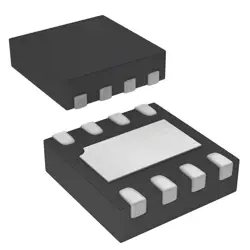
이미지는 참조용만
GD25LQ40EEIGR
IC FLASH 4MBIT SPI/QUAD 8USON
- 제조업체
- Mfr.부분 #GD25LQ40EEIGR
- 패키지
- 데이터시트
- 재고 있음28711
100% 원래 &새로운
배송 준비 24 시간
365 일 보장
RFQ 및더 많은 할인
사양
| Series | GD25LQ |
| Part Status | Active |
| Base Product Number | GD25LQ40 |
| Memory Type | Non-Volatile |
| Memory Format | FLASH |
| Technology | FLASH - NOR (SLC) |
| Memory Size | 4Mbit |
| Memory Organization | 512K x 8 |
| Memory Interface | SPI - Quad I/O |
| Clock Frequency | 133 MHz |
| Write Cycle Time - Word, Page | 60µs, 2.4ms |
| Voltage - Supply | 1.65V ~ 2V |
| Operating Temperature | -40°C ~ 85°C (TA) |
| Mounting Type | Surface Mount |
| Package | 8-XFDFN Exposed Pad |
| Supplier Device Package | 8-USON (3x2) |
| Packaging | Cut Tape (CT), Tape & Reel (TR) |
| Access Time | 6 ns |
개요
Description
Key features (typical): standard SPI read/write/erase commands, fast read, page programming (usually 256 bytes), sector/block erase options, and deep power‑down with resume. It supports higher‑speed Quad I/O reads for faster data transfer and provides hardware write protection. Operating voltage and exact timing depend on the specific variant, but industrial‑grade parts are designed for robust operation in harsher environments.
Typical uses: boot code storage for microcontrollers, firmware updates, and data storage in embedded applications where a small, non‑volatile memory is required.
For precise electrical specs, available interfaces, timings, and packaging details, consult the GD25LQ40E/GD25LQ40EE datasheet and the IGR packaging spec.
Features
- Capacity: 4 Mbit (512 KB)
- Interface: Serial SPI with Dual/Quad I/O read support
- Voltage: 2.7–3.6 V operation
- Addressing: 24-bit address
- Page size: 256 bytes; Page program
- Erase: 4 KB sectors, 64 KB blocks, and chip erase
- Speeds: High-speed read modes; Quad IO reads for higher throughput
- Features: Deep power-down, WP#/HOLD# pins, basic security features with block protection
- Endurance/Retention: ~100k P/E cycles; data retention >20 years
- Temperature: Industrial range (-40°C to 85°C)
- Packaging: 8-pin GR (SOP-8)
Ideal for code/data storage in embedded systems requiring small footprint, low voltage, and basic security/protection.
Package
Pinout
- Function: SPI serial flash memory (non-volatile storage). Pins typically: 1 CS, 2 DO (MISO), 3 WP, 4 GND, 5 DI (MOSI), 6 CLK, 7 HOLD, 8 VCC.
Manufacturer
- What kind of company: A semiconductor company specializing in non-volatile memory products, notably serial NOR/NAND flash memory and related IC solutions.
Application
- MCU boot flash and firmware storage in embedded systems
- Firmware updates/storage for consumer electronics, IoT, and industrial equipment
- Code/data memory for wearables and portable devices
- Data logging memory in industrial controllers, meters, and networking gear
- Compact automotive ECU firmware memory for small-scale systems
Equivalent
- Winbond W25Q40BV/BV(E)
- Macronix MX25LQ040 (MX25LQ040/MX25LQ040E)
- Everspin/EC EN25Q40B
- Spansion (Cypress) S25FL040
- ISSI IS25LP040D
- Microchip/Atmel AT25DF040A
Note: pinout and timing vary by vendor; verify exact package and timing before substitution.
배송
배송 방법We
DHL, FedEx, TNT, UPS 또는 선택한 다른 운송업체를 통해 글로벌 배송 서비스를 제공합니다.
배송 요금 참조 (DHL/FedEx):
DHL은: 배송 비용은 $25-$45 (0.5kg)에서 2-5 영업일의 추정적 배달 시간이 있습니다.
FedEx는: 배송 비용은 $25-$40 (0.5kg)에서 3-7 영업일의 추정적 배달 시간을 가지고 있습니다.
UPS는: 배송 비용은 $25-$45 (0.5kg)에서 3-7 영업일의 추정적 배달 시간을 가지고 있습니다.
TNT는: 배송 비용은 $25-$65 (0.5kg)에서 3-7 영업일의 추정적 배달 시간을 가지고 있습니다.
EMS는: 배송 비용은 $30-$50 (0.5kg)에서 7-15 영업일의 추정적 배달 시간을 제공합니다.
등록된 항공우편: 배송 비용은 $2-$4 (0.1kg), 예상 배달 시간 5-20 영업일.
지불
Payment Methods
지불 기간은 100% 사전 지불입니다.
현재, 우리는 아래 지불 방법만 받아들입니다.:
1. PayPal
2. 신용/직불 카드
3. 전선 전송
비슷한
-
![MX25R8035FM1IL0]() MX25R8035FM1IL0
Macronix
-
![MX25V5126FM1I]() MX25V5126FM1I
Macronix
-
![MX25V4035FZUI]() MX25V4035FZUI
Macronix
-
![MX25R3235FZNIL0]() MX25R3235FZNIL0
Macronix
-
![MX25R6435FBDIL0]() MX25R6435FBDIL0
Macronix
-
![MX25L25673GMI-10G]() MX25L25673GMI-10G
Macronix
-
![MX25V1635FM2I]() MX25V1635FM2I
Macronix
-
![MX25U3232FZBI02]() MX25U3232FZBI02
Macronix
-
![MX25L12833FZNI-10G]() MX25L12833FZNI-10..
Macronix
-
![MX29F040CQI-70G]() MX29F040CQI-70G
Macronix
-
![MX25L25645GXDI-08G]() MX25L25645GXDI-08..
Macronix
-
![MX29F040CTI-70G]() MX29F040CTI-70G
Macronix