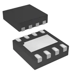
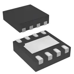
이미지는 참조용만
GD25LQ64CWIGR
IC FLASH 64MBIT SPI/QUAD 8WSON
- 제조업체
- Mfr.부분 #GD25LQ64CWIGR
- 패키지
- 데이터시트
- 재고 있음5753
100% 원래 &새로운
배송 준비 24 시간
365 일 보장
RFQ 및더 많은 할인
사양
| Part Status | Obsolete |
| DigiKey Programmable | Not Verified |
| Memory Type | Non-Volatile |
| Memory Format | FLASH |
| Technology | FLASH - NOR |
| Memory Size | 64Mbit |
| Memory Organization | 8M x 8 |
| Memory Interface | SPI - Quad I/O |
| Clock Frequency | 120 MHz |
| Write Cycle Time - Word, Page | 2.4ms |
| Voltage - Supply | 1.65V ~ 2V |
| Operating Temperature | -40°C ~ 85°C (TA) |
| Mounting Type | Surface Mount |
| Package / Case | 8-WDFN Exposed Pad |
| Supplier Device Package | 8-WSON (5x6) |
| Base Product Number | GD25LQ64 |
개요
Description
This memory chip offers features such as fast random access, low power consumption, and a wide temperature range, making it suitable for embedded systems, consumer electronics, and automotive applications. It also supports a range of commands for reading, writing, and erasing data, with a typical erase time of around 0.5 seconds for a sector.
The GD25LQ64CWIGR is packaged in a compact 8-lead SOIC or 16-lead WSON format, facilitating integration into various designs. Its robust performance and reliability make it a popular choice among developers for applications requiring non-volatile memory storage.
Features
1. Interface: SPI (Serial Peripheral Interface) with modes up to 104 MHz for fast data transfer.
2. Memory Organization: 64 Megabits organized as 8M x 8, allowing for efficient storage and retrieval of data.
3. Voltage Range: Operates at a supply voltage of 2.7V to 3.6V, suitable for low-power applications.
4. Data Retention: Offers a data retention period of up to 20 years, ensuring long-term reliability.
5. Programming and Erasing: Supports 4KB sector erase, 32KB block erase, and full chip erase capabilities for flexible memory management.
6. High-Performance: Read speeds of up to 85 MB/s, enabling quick access to stored data.
7. Packages: Available in various package options, including SOIC, WSON, and DFN, facilitating integration into different designs.
This device is ideal for applications requiring reliable, high-speed data storage with low power consumption.
Package
Pinout
### Pin Functions:
1. VCC: Power supply pin.
2. GND: Ground pin.
3. SO (Serial Output): Data output pin for read operations.
4. SI (Serial Input): Data input pin for write operations.
5. SCK (Serial Clock): Clock input for synchronous communication.
6. CS# (Chip Select): Active low pin to enable the device.
7. WP# (Write Protect): Active low pin to protect against write operations.
8. HOLD#: Active low pin to pause operations without resetting the device.
This device supports standard and dual I/O SPI interfaces for data transfer.
Manufacturer
Application
Equivalent
배송
배송 방법We
DHL, FedEx, TNT, UPS 또는 선택한 다른 운송업체를 통해 글로벌 배송 서비스를 제공합니다.
배송 요금 참조 (DHL/FedEx):
DHL은: 배송 비용은 $25-$45 (0.5kg)에서 2-5 영업일의 추정적 배달 시간이 있습니다.
FedEx는: 배송 비용은 $25-$40 (0.5kg)에서 3-7 영업일의 추정적 배달 시간을 가지고 있습니다.
UPS는: 배송 비용은 $25-$45 (0.5kg)에서 3-7 영업일의 추정적 배달 시간을 가지고 있습니다.
TNT는: 배송 비용은 $25-$65 (0.5kg)에서 3-7 영업일의 추정적 배달 시간을 가지고 있습니다.
EMS는: 배송 비용은 $30-$50 (0.5kg)에서 7-15 영업일의 추정적 배달 시간을 제공합니다.
등록된 항공우편: 배송 비용은 $2-$4 (0.1kg), 예상 배달 시간 5-20 영업일.
지불
Payment Methods
지불 기간은 100% 사전 지불입니다.
현재, 우리는 아래 지불 방법만 받아들입니다.:
1. PayPal
2. 신용/직불 카드
3. 전선 전송
비슷한
-
![MX25L3233FZBI-08Q]() MX25L3233FZBI-08Q
Macronix
-
![MX25V1635FZNQ03]() MX25V1635FZNQ03
Macronix
-
![MX66U1G45GXDI00]() MX66U1G45GXDI00
Macronix
-
![MX25V2033FM1I]() MX25V2033FM1I
Macronix
-
![MX30LF2G28AD-TI]() MX30LF2G28AD-TI
Macronix
-
![MX25L25673GMI-08G]() MX25L25673GMI-08G
Macronix
-
![MX25U51279GXDR00]() MX25U51279GXDR00
Macronix
-
![MX25L2006EM1I-12G]() MX25L2006EM1I-12G
Macronix
-
![MX25R1635FZUIH0]() MX25R1635FZUIH0
Macronix
-
![MX25V1635FM2I]() MX25V1635FM2I
Macronix
-
![MX25U3232FZBI02]() MX25U3232FZBI02
Macronix
-
![MX25L6433FM2I-08G]() MX25L6433FM2I-08G
Macronix