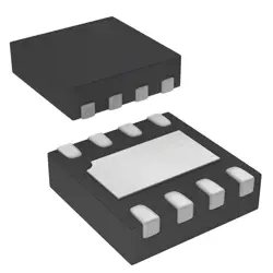
이미지는 참조용만
IS42S16320F-6TLI
IC DRAM 512MBIT PAR 54TSOP II
- 제조업체
- Mfr.부분 #IS42S16320F-6TLI
- 패키지
- 데이터시트 IS42S16320F-6TLI DataSheet
- 재고 있음7989
100% 원래 &새로운
배송 준비 24 시간
365 일 보장
RFQ 및더 많은 할인
사양
| Part Status | Active |
| DigiKey Programmable | Not Verified |
| Memory Type | Volatile |
| Memory Format | DRAM |
| Technology | SDRAM |
| Memory Size | 512Mbit |
| Memory Organization | 32M x 16 |
| Memory Interface | Parallel |
| Clock Frequency | 167 MHz |
| Access Time | 5.4 ns |
| Voltage - Supply | 3V ~ 3.6V |
| Operating Temperature | -40°C ~ 85°C (TA) |
| Mounting Type | Surface Mount |
| Package / Case | 54-TSOP (0.400", 10.16mm Width) |
| Supplier Device Package | 54-TSOP II |
| Base Product Number | IS42S16320 |
개요
Description
The chip is organized as 16 bits x 16 banks and utilizes a 3.3V power supply. It features pipelined architecture, allowing for fast access times and enabling high-speed data processing required in applications like consumer electronics, networking equipment, and computing devices. The device is housed in a compact TSOP II package, making it suitable for space-constrained designs.
Overall, the IS42S16320F-6TLI is widely utilized for its reliability and efficiency in various electronic applications, contributing significantly to system performance enhancement.
Features
1. Organization: It is organized as 256K x 16 bits, allowing efficient data handling.
2. Speed: Operates at a memory clock frequency of up to 400 MHz, with a corresponding data rate of 800 MT/s.
3. Voltage: Designed to operate at a low voltage of 1.8V, which helps in reducing power consumption.
4. Package: Available in a 54-ball TFBGA (Thin Fine Ball Grid Array) package, ensuring a compact design suitable for various applications.
5. Burst Mode: Supports burst lengths of 4 and 8, enhancing performance for sequential data access.
6. Latency: Features a CAS latency of 6 cycles, optimizing speed for various applications.
7. Applications: Suitable for use in consumer electronics, networking equipment, and industrial applications requiring reliable and high-speed memory.
These features make the IS42S16320F-6TLI a versatile choice for various high-performance memory applications.
Package
Pinout
The primary functions of the pins include:
1. Data Pins (DQ0-DQ31): These are used for bi-directional data transfer.
2. Address Pins (A0-A11): These determine the address of the memory location being accessed.
3. Control Pins (CLK, CKE, CS, RAS, CAS, WE): These manage the timing and control of read/write operations.
4. Byte Enable Pins (BW0-BW3): These enable writing to specific bytes in the memory.
5. Power and Ground Pins (VDD, VSS): Provide the necessary power supply and ground reference.
This chip operates with a supply voltage of 3.3V and is commonly used in various applications requiring high-density memory solutions.
Manufacturer
Application
Equivalent
배송
배송 방법We
DHL, FedEx, TNT, UPS 또는 선택한 다른 운송업체를 통해 글로벌 배송 서비스를 제공합니다.
배송 요금 참조 (DHL/FedEx):
DHL은: 배송 비용은 $25-$45 (0.5kg)에서 2-5 영업일의 추정적 배달 시간이 있습니다.
FedEx는: 배송 비용은 $25-$40 (0.5kg)에서 3-7 영업일의 추정적 배달 시간을 가지고 있습니다.
UPS는: 배송 비용은 $25-$45 (0.5kg)에서 3-7 영업일의 추정적 배달 시간을 가지고 있습니다.
TNT는: 배송 비용은 $25-$65 (0.5kg)에서 3-7 영업일의 추정적 배달 시간을 가지고 있습니다.
EMS는: 배송 비용은 $30-$50 (0.5kg)에서 7-15 영업일의 추정적 배달 시간을 제공합니다.
등록된 항공우편: 배송 비용은 $2-$4 (0.1kg), 예상 배달 시간 5-20 영업일.
지불
Payment Methods
지불 기간은 100% 사전 지불입니다.
현재, 우리는 아래 지불 방법만 받아들입니다.:
1. PayPal
2. 신용/직불 카드
3. 전선 전송
비슷한
-
![MX66U1G45GXDI00]() MX66U1G45GXDI00
Macronix
-
![MX25V16066M1I02]() MX25V16066M1I02
Macronix
-
![MX25V16066M2I02]() MX25V16066M2I02
Macronix
-
![MX30LF2G28AD-TI]() MX30LF2G28AD-TI
Macronix
-
![MX25U25643GZNI00]() MX25U25643GZNI00
Macronix
-
![MX25L2006EM1I-12G]() MX25L2006EM1I-12G
Macronix
-
![MX25R1635FZUIH0]() MX25R1635FZUIH0
Macronix
-
![MX25U3232FZBI02]() MX25U3232FZBI02
Macronix
-
![MX25L12833FM2I-10G]() MX25L12833FM2I-10..
Macronix
-
![MX25L12833FZ2I-10G]() MX25L12833FZ2I-10..
Macronix
-
![MX25L12833FZNI-10G]() MX25L12833FZNI-10..
Macronix
-
![MX25U25645GXDI00]() MX25U25645GXDI00
Macronix