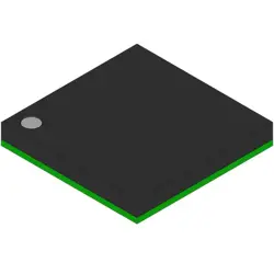
이미지는 참조용만
IS42S16400J-7BLI
IC DRAM 64MBIT PAR 54TFBGA
- 제조업체
- Mfr.부분 #IS42S16400J-7BLI
- 패키지
- 데이터시트 IS42S16400J-7BLI DataSheet
- 재고 있음9313
100% 원래 &새로운
배송 준비 24 시간
365 일 보장
RFQ 및더 많은 할인
사양
| Part Status | Obsolete |
| DigiKey Programmable | Not Verified |
| Memory Type | Volatile |
| Memory Format | DRAM |
| Technology | SDRAM |
| Memory Size | 64Mbit |
| Memory Organization | 4M x 16 |
| Memory Interface | Parallel |
| Voltage - Supply | 3V ~ 3.6V |
| Operating Temperature | -40°C ~ 85°C (TA) |
| Mounting Type | Surface Mount |
| Package / Case | 54-TFBGA |
| Supplier Device Package | 54-TFBGA (8x8) |
| Base Product Number | IS42S16400 |
| Clock Frequency | 143 MHz |
| Access Time | 5.4 ns |
개요
Description
Key specifications include a data rate of 7.5 ns, allowing for efficient data transfer, and an operational voltage of 2.5V, which helps reduce power consumption. The chip supports standard SDRAM commands and operates in a synchronous manner, allowing for improved performance through pipelining and burst access modes.
The "7BLI" designation indicates specific characteristics such as temperature range and packaging type. Overall, the IS42S16400J-7BLI is designed to meet the demands of modern electronic systems with a focus on speed and efficiency.
Features
- Speed: Operates at a clock frequency of up to 143 MHz with a low latency (7.5 ns).
- Power Supply: Requires a core voltage of 2.5V, with I/O voltage typically at 2.5V or 3.3V.
- Interface: Supports a synchronous interface, enabling better performance and timing control.
- Access Time: Fast access time suitable for various applications in consumer electronics and computing.
- Package: Available in a 54-pin TSOP-II package, facilitating easy integration into printed circuit boards.
- Data Rate: Capable of high data transfer rates due to its synchronous operation and pipelined architecture.
This memory chip is commonly used in applications such as digital TVs, set-top boxes, and other consumer electronics requiring reliable, high-speed memory solutions.
Package
Pinout
1. Address Pins (A0-A18): Used to select the memory location to read from or write to.
2. Data Pins (D0-D3): Used for input and output of 4 bits of data.
3. Chip Enable (CE): Activates the chip for read or write operations.
4. Write Enable (WE): Controls write operations; when low, data can be written.
5. Output Enable (OE): Enables data output when low.
6. Ground (VSS): Provides the ground reference.
7. Power Supply (VDD): Supplies power to the chip.
This SRAM operates with a fast access time and is suitable for various applications, including caching and buffers in electronic devices.
Manufacturer
Application
Equivalent
1. MT48LC16M4A2P-75 - Micron Technology
2. K4S641632D-7 - Samsung
3. HY57V641620BTP - Hynix
Always verify compatibility based on specifications such as timing, voltage, and package type.
배송
배송 방법We
DHL, FedEx, TNT, UPS 또는 선택한 다른 운송업체를 통해 글로벌 배송 서비스를 제공합니다.
배송 요금 참조 (DHL/FedEx):
DHL은: 배송 비용은 $25-$45 (0.5kg)에서 2-5 영업일의 추정적 배달 시간이 있습니다.
FedEx는: 배송 비용은 $25-$40 (0.5kg)에서 3-7 영업일의 추정적 배달 시간을 가지고 있습니다.
UPS는: 배송 비용은 $25-$45 (0.5kg)에서 3-7 영업일의 추정적 배달 시간을 가지고 있습니다.
TNT는: 배송 비용은 $25-$65 (0.5kg)에서 3-7 영업일의 추정적 배달 시간을 가지고 있습니다.
EMS는: 배송 비용은 $30-$50 (0.5kg)에서 7-15 영업일의 추정적 배달 시간을 제공합니다.
등록된 항공우편: 배송 비용은 $2-$4 (0.1kg), 예상 배달 시간 5-20 영업일.
지불
Payment Methods
지불 기간은 100% 사전 지불입니다.
현재, 우리는 아래 지불 방법만 받아들입니다.:
1. PayPal
2. 신용/직불 카드
3. 전선 전송
비슷한
-
![MX25R8035FM1IL0]() MX25R8035FM1IL0
Macronix
-
![MX29F400CBTI-70G]() MX29F400CBTI-70G
Macronix
-
![MX25V2033FM1I]() MX25V2033FM1I
Macronix
-
![MX29GL512FHXFI-11G]() MX29GL512FHXFI-11..
Macronix
-
![MX25U51279GXDR00]() MX25U51279GXDR00
Macronix
-
![MX25R1635FZUIH0]() MX25R1635FZUIH0
Macronix
-
![MX25V1635FM2I]() MX25V1635FM2I
Macronix
-
![MX25U3232FZBI02]() MX25U3232FZBI02
Macronix
-
![MX25L6433FM2I-08G]() MX25L6433FM2I-08G
Macronix
-
![MX25L12833FM2I-10G]() MX25L12833FM2I-10..
Macronix
-
![MX25U25645GXDI00]() MX25U25645GXDI00
Macronix
-
![MX25L12835FZ2I-10G]() MX25L12835FZ2I-10..
Macronix