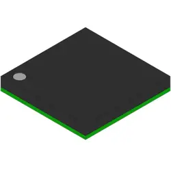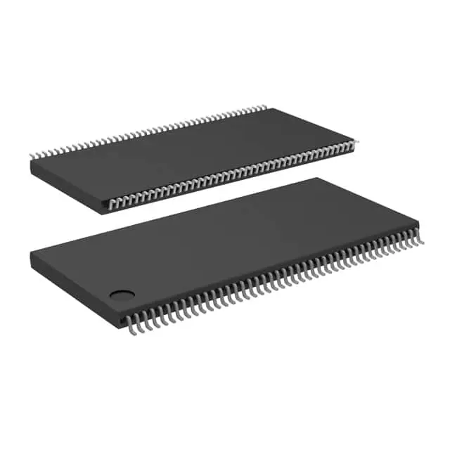
이미지는 참조용만
IS42S32800D-6TLI
IC DRAM 256MBIT PAR 86TSOP II
- 제조업체
- Mfr.부분 #IS42S32800D-6TLI
- 패키지 86-TFSOP (0.400", 10.16mm Width)
- 데이터시트
- 재고 있음3658
100% 원래 &새로운
배송 준비 24 시간
365 일 보장
RFQ 및더 많은 할인
사양
| Package | Tray |
| ProductStatus | Obsolete |
| MemoryType | Volatile |
| MemoryFormat | DRAM |
| Technology | SDRAM |
| MemorySize | 256Mb (8M x 32) |
| MemoryInterface | Parallel |
| ClockFrequency | 166 MHz |
| AccessTime | 5.4 ns |
| Voltage-Supply | 3V ~ 3.6V |
| OperatingTemperature | -40°C ~ 85°C (TA) |
| MountingType | Surface Mount |
| Package/Case | 86-TFSOP (0.400, 10.16mm Width) |
개요
Description
Key characteristics include a speed grade of 6 ns, making it suitable for various applications requiring fast access times, such as consumer electronics, networking equipment, and industrial products. The chip supports various modes of operation, including burst mode for efficient data handling. Additionally, it incorporates a slew of features to enhance performance and reliability, including deep power-down modes and low standby current consumption.
The IS42S32800D-6TLI is commonly used in systems where compact memory solutions are crucial, offering a blend of performance and efficiency.
Features
1. Organization: It is organized as 4M x 8 bits.
2. Speed: Operates at a clock frequency of 166 MHz (6 ns cycle time), making it suitable for high-performance applications.
3. Voltage Supply: It operates on a core voltage of 2.5V.
4. Interface: Supports a double data rate (DDR) interface, enabling faster data processing by transferring data on both rising and falling edges of the clock signal.
5. Data Rate: Achieves a data rate of up to 333 Mbps per pin.
6. Package: Typically available in a 54-ball FBGA (Fine Ball Grid Array) package.
7. Applications: Commonly used in digital consumer applications, networking devices, and automotive electronics.
Overall, the IS42S32800D-6TLI is designed for efficiency and speed, making it a reliable choice for embedded systems and high-speed computing applications.
Package
Pinout
Key pin functions are:
- VDD: Power supply for the chip.
- VSS: Ground connection.
- DQ[0:31]: Data input/output lines for transferring data.
- A[0:25]: Address lines for selecting memory locations.
- BA[0:1]: Bank address lines to select the bank.
- CLK: Clock input for synchronization.
- CS: Chip select for enabling/disabling the chip.
- WE: Write enable signal for write operations.
- CAS: Column address strobe for read operations.
- RAS: Row address strobe for activating rows.
This chip is used in various applications requiring high-density memory solutions.
Manufacturer
Application
Equivalent
1. MT47H128M8 - Micron
2. K4T1G164QE - Samsung
3. H5TQ2G83AFR - Hynix
These alternatives have similar specifications and can be used in compatible applications. Always verify specific pin configurations and electrical characteristics before substitution.
배송
배송 방법We
DHL, FedEx, TNT, UPS 또는 선택한 다른 운송업체를 통해 글로벌 배송 서비스를 제공합니다.
배송 요금 참조 (DHL/FedEx):
DHL은: 배송 비용은 $25-$45 (0.5kg)에서 2-5 영업일의 추정적 배달 시간이 있습니다.
FedEx는: 배송 비용은 $25-$40 (0.5kg)에서 3-7 영업일의 추정적 배달 시간을 가지고 있습니다.
UPS는: 배송 비용은 $25-$45 (0.5kg)에서 3-7 영업일의 추정적 배달 시간을 가지고 있습니다.
TNT는: 배송 비용은 $25-$65 (0.5kg)에서 3-7 영업일의 추정적 배달 시간을 가지고 있습니다.
EMS는: 배송 비용은 $30-$50 (0.5kg)에서 7-15 영업일의 추정적 배달 시간을 제공합니다.
등록된 항공우편: 배송 비용은 $2-$4 (0.1kg), 예상 배달 시간 5-20 영업일.
지불
Payment Methods
지불 기간은 100% 사전 지불입니다.
현재, 우리는 아래 지불 방법만 받아들입니다.:
1. PayPal
2. 신용/직불 카드
3. 전선 전송
비슷한
-
![MX25L3233FZBI-08Q]() MX25L3233FZBI-08Q
Macronix
-
![MX25L3233FM1I-08Q]() MX25L3233FM1I-08Q
Macronix
-
![MX66U1G45GXDI00]() MX66U1G45GXDI00
Macronix
-
![MX25V2033FM1I]() MX25V2033FM1I
Macronix
-
![MX25V16066M1I02]() MX25V16066M1I02
Macronix
-
![MX25L8035EM2I-10G]() MX25L8035EM2I-10G
Macronix
-
![MX29GL512FHXFI-11G]() MX29GL512FHXFI-11..
Macronix
-
![MX25L2006EM1I-12G]() MX25L2006EM1I-12G
Macronix
-
![MX25U6435FM2I-10G]() MX25U6435FM2I-10G
Macronix
-
![MX25L12833FM2I-10G]() MX25L12833FM2I-10..
Macronix
-
![MX25L12833FZNI-10G]() MX25L12833FZNI-10..
Macronix
-
![MX25U25645GXDI00]() MX25U25645GXDI00
Macronix