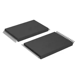
이미지는 참조용만
IS43TR16256A-15HBLI
IC DRAM 4GBIT PARALLEL 96TWBGA
- 제조업체
- Mfr.부분 #IS43TR16256A-15HBLI
- 패키지 BGA-96
- 데이터시트
- 재고 있음3880
100% 원래 &새로운
배송 준비 24 시간
365 일 보장
RFQ 및더 많은 할인
사양
| Package | Tray |
| ProductStatus | Obsolete |
| MemoryType | Volatile |
| MemoryFormat | DRAM |
| Technology | SDRAM - DDR3 |
| MemorySize | 4Gb (256M x 16) |
| MemoryInterface | Parallel |
| ClockFrequency | 667 MHz |
| WriteCycleTime-WordPage | 15ns |
| AccessTime | 20 ns |
| Voltage-Supply | 1.425V ~ 1.575V |
| OperatingTemperature | -40°C ~ 95°C (TC) |
| MountingType | Surface Mount |
| Package/Case | 96-TFBGA |
개요
Description
The "-15" in the part number indicates a maximum clock frequency of 1,333 MHz with a data transfer rate of 1,066 MT/s (megatransfers per second). The "BLI" suffix suggests specific package types or temperature grades. This memory chip operates at a voltage of 1.5V, contributing to its energy efficiency.
Key features include a flexible burst length, support for a range of operating temperatures, and compatibility with standard DDR3 interfaces. It is widely used in applications that require high-speed data access and reliability, such as laptops, desktops, and networking equipment. The IS43TR16256A-15HBLI enhances system performance and responsiveness in data-intensive environments.
Features
- Density: 256 Megabits organized as 32 Meg x 8 bits.
- Speed: Operates at a clock frequency of 400 MHz, with a data transfer rate of up to 800 MT/s.
- Interface: DDR2 interface, supporting a 4-bit prefetch architecture.
- Power Supply: Operates at 1.8V, with low power consumption compared to earlier DDR technologies.
- Package: Typically available in a 60-ball FBGA (Fine Ball Grid Array) package.
- Latency: Offers a CAS latency of 5, enhancing performance in various applications.
- Temperature Range: Suitable for industrial and commercial environments.
- Applications: Ideal for use in networking, telecommunications, and consumer electronics.
This memory chip is optimized for high-speed data processing and efficient power usage, making it a reliable choice for modern electronic devices.
Package
Pinout
1. Data Input/Output: 16 data lines (DQ0-DQ15) for data transfer.
2. Address Inputs: 13 address lines (A0-A12) for selecting memory addresses.
3. Control Signals:
- CS (Chip Select): Activates the memory chip.
- CKE (Clock Enable): Activates or deactivates the clock.
- CLK (Clock): Synchronizes operations.
- RAS (Row Address Strobe), CAS (Column Address Strobe), and WE (Write Enable): Control read and write operations.
4. Power and Ground: VDD and VSS for power supply and ground connections.
5. Burst Length: Controls the burst length of the memory operation.
This combination of pins allows the chip to perform high-speed memory operations in a synchronous manner, suitable for various applications in computing and embedded systems.
Manufacturer
Application
Equivalent
1. MT41J256M16HA-15E
2. H5TQ2G83BFR
3. K4B4G1646F
Always verify compatibility based on specific application requirements, voltage levels, and timing parameters before substitution.
배송
배송 방법We
DHL, FedEx, TNT, UPS 또는 선택한 다른 운송업체를 통해 글로벌 배송 서비스를 제공합니다.
배송 요금 참조 (DHL/FedEx):
DHL은: 배송 비용은 $25-$45 (0.5kg)에서 2-5 영업일의 추정적 배달 시간이 있습니다.
FedEx는: 배송 비용은 $25-$40 (0.5kg)에서 3-7 영업일의 추정적 배달 시간을 가지고 있습니다.
UPS는: 배송 비용은 $25-$45 (0.5kg)에서 3-7 영업일의 추정적 배달 시간을 가지고 있습니다.
TNT는: 배송 비용은 $25-$65 (0.5kg)에서 3-7 영업일의 추정적 배달 시간을 가지고 있습니다.
EMS는: 배송 비용은 $30-$50 (0.5kg)에서 7-15 영업일의 추정적 배달 시간을 제공합니다.
등록된 항공우편: 배송 비용은 $2-$4 (0.1kg), 예상 배달 시간 5-20 영업일.
지불
Payment Methods
지불 기간은 100% 사전 지불입니다.
현재, 우리는 아래 지불 방법만 받아들입니다.:
1. PayPal
2. 신용/직불 카드
3. 전선 전송
비슷한
-
![MX25V1635FZNI]() MX25V1635FZNI
Macronix
-
![MX66U1G45GXDI00]() MX66U1G45GXDI00
Macronix
-
![MX25V4035FZUI]() MX25V4035FZUI
Macronix
-
![MX25R3235FZNIL0]() MX25R3235FZNIL0
Macronix
-
![MX30LF2G28AD-TI]() MX30LF2G28AD-TI
Macronix
-
![MX25L25673GMI-10G]() MX25L25673GMI-10G
Macronix
-
![MX25R1635FZUIH0]() MX25R1635FZUIH0
Macronix
-
![MX25L12833FZ2I-10G]() MX25L12833FZ2I-10..
Macronix
-
![MX29LV160DTTI-70G]() MX29LV160DTTI-70G
Macronix
-
![MX25L25645GXDI-08G]() MX25L25645GXDI-08..
Macronix
-
![MX29F040CTI-70G]() MX29F040CTI-70G
Macronix
-
![MX29F800CBTI-70G]() MX29F800CBTI-70G
Macronix