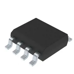
이미지는 참조용만
IS45S16320F-6TLA1
IC DRAM 512MBIT PAR 54TSOP II
- 제조업체
- Mfr.부분 #IS45S16320F-6TLA1
- 패키지
- 데이터시트
- 재고 있음8981
100% 원래 &새로운
배송 준비 24 시간
365 일 보장
RFQ 및더 많은 할인
사양
| Part Status | Active |
| DigiKey Programmable | Not Verified |
| Memory Type | Volatile |
| Memory Format | DRAM |
| Technology | SDRAM |
| Memory Size | 512Mbit |
| Memory Organization | 32M x 16 |
| Memory Interface | Parallel |
| Voltage - Supply | 3V ~ 3.6V |
| Operating Temperature | -40°C ~ 85°C (TA) |
| Mounting Type | Surface Mount |
| Package / Case | 54-TSOP (0.400", 10.16mm Width) |
| Supplier Device Package | 54-TSOP II |
| Base Product Number | IS45S16320 |
| Clock Frequency | 167 MHz |
| Access Time | 5.4 ns |
개요
Description
This memory chip supports a range of operating frequencies, typically up to 133 MHz, with a fast access time, which makes it advantageous for applications requiring quick data retrieval. The IS45S16320F-6TLA1 is designed for use in consumer electronics, such as mobile devices, automotive systems, and industrial applications, where reliability and efficiency are critical. The "6TLA1" in its designation indicates specific packaging and operational parameters, ensuring that it meets the requirements of modern electronic designs. Overall, the IS45S16320F-6TLA1 is a versatile and reliable memory solution suited for diverse applications in today's technology landscape.
Features
1. Memory Configuration: 16 Meg x 32 bits, allowing for a total of 64 Megabytes of memory.
2. Speed Grade: Operates at a clock frequency of up to 166 MHz, suitable for high-speed data processing.
3. Interface: Synchronous interface that provides high bandwidth and low latency.
4. Power Supply: Operates at a low voltage of 3.3V, enhancing energy efficiency.
5. Burst Length: Supports burst lengths of 1, 2, 4, and 8, allowing for flexible data transfer rates.
6. Package Type: Available in a 54-pin TSOP II package, making it suitable for various PCB designs.
7. Temperature Range: Typically rated for industrial temperature ranges, ensuring reliability in various environments.
This chip is ideal for applications requiring fast data access and reliable performance, such as telecommunications, networking equipment, and embedded systems.
Package
Pinout
The primary functions of the pins include:
- Data Pins (DQ0-DQ15): Data inputs/outputs for reading and writing data.
- Address Pins (A0-A11): To select rows and columns within the memory banks.
- Control Pins (CS, RAS, CAS, WE): For chip selection, row address strobe, column address strobe, and write enable functions.
- Clock Pins (CLK, CLK_B): For synchronizing data transfers.
- Power Supply Pins (VDD, VSS): For power supply and ground connections.
This device typically operates at clock speeds up to 166 MHz and is used in various applications requiring high-speed memory access.
Manufacturer
Application
Equivalent
1. MT41K256M16HA-125
2. H5TQ1G83CFR
3. K4B4G1646D-BCK0
Ensure to check specifications like voltage, speed, and package type for compatibility.
배송
배송 방법We
DHL, FedEx, TNT, UPS 또는 선택한 다른 운송업체를 통해 글로벌 배송 서비스를 제공합니다.
배송 요금 참조 (DHL/FedEx):
DHL은: 배송 비용은 $25-$45 (0.5kg)에서 2-5 영업일의 추정적 배달 시간이 있습니다.
FedEx는: 배송 비용은 $25-$40 (0.5kg)에서 3-7 영업일의 추정적 배달 시간을 가지고 있습니다.
UPS는: 배송 비용은 $25-$45 (0.5kg)에서 3-7 영업일의 추정적 배달 시간을 가지고 있습니다.
TNT는: 배송 비용은 $25-$65 (0.5kg)에서 3-7 영업일의 추정적 배달 시간을 가지고 있습니다.
EMS는: 배송 비용은 $30-$50 (0.5kg)에서 7-15 영업일의 추정적 배달 시간을 제공합니다.
등록된 항공우편: 배송 비용은 $2-$4 (0.1kg), 예상 배달 시간 5-20 영업일.
지불
Payment Methods
지불 기간은 100% 사전 지불입니다.
현재, 우리는 아래 지불 방법만 받아들입니다.:
1. PayPal
2. 신용/직불 카드
3. 전선 전송
비슷한
-
![MX25L3233FM1I-08Q]() MX25L3233FM1I-08Q
Macronix
-
![MX66U1G45GXDI00]() MX66U1G45GXDI00
Macronix
-
![MX25V4035FZUI]() MX25V4035FZUI
Macronix
-
![MX25V2033FM1I]() MX25V2033FM1I
Macronix
-
![MX25R6435FBDIL0]() MX25R6435FBDIL0
Macronix
-
![MX25L25673GMI-10G]() MX25L25673GMI-10G
Macronix
-
![MX25V1635FM2I]() MX25V1635FM2I
Macronix
-
![MX25L6433FM2I-08G]() MX25L6433FM2I-08G
Macronix
-
![MX25U6435FM2I-10G]() MX25U6435FM2I-10G
Macronix
-
![MX25L12833FZ2I-10G]() MX25L12833FZ2I-10..
Macronix
-
![MX25U25645GXDI00]() MX25U25645GXDI00
Macronix
-
![MX25L12835FZ2I-10G]() MX25L12835FZ2I-10..
Macronix