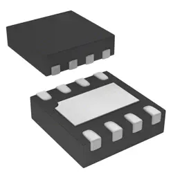
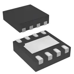
이미지는 참조용만
IS61WV102416BLL-10TLI
IC SRAM 16MBIT PARALLEL 48TSOP I
- 제조업체
- Mfr.부분 #IS61WV102416BLL-10TLI
- 패키지 SOP-48
- 데이터시트 IS61WV102416BLL-10TLI DataSheet
- 재고 있음6675
100% 원래 &새로운
배송 준비 24 시간
365 일 보장
RFQ 및더 많은 할인
사양
| Package | Tray |
| ProductStatus | Active |
| MemoryType | Volatile |
| MemoryFormat | SRAM |
| Technology | SRAM - Asynchronous |
| MemorySize | 16Mb (1M x 16) |
| MemoryInterface | Parallel |
| WriteCycleTime-WordPage | 10ns |
| AccessTime | 10 ns |
| Voltage-Supply | 2.4V ~ 3.6V |
| OperatingTemperature | -40°C ~ 85°C (TA) |
| MountingType | Surface Mount |
| Package/Case | 48-TFSOP (0.724, 18.40mm Width) |
개요
Description
This SRAM is known for its fast access times, with a maximum access time of 10 nanoseconds, which is ideal for high-speed applications. The chip supports asynchronous read and write operations, enhancing its usability in dynamic environments. It also includes features like a tri-state output, making it easy to integrate into systems with multiple data sources.
Due to its compact design, low power consumption, and high-speed performance, the IS61WV102416BLL-10TLI is commonly used in consumer electronics, telecommunications, automotive, and industrial applications.
Features
1. Organization: 2M x 8-bit configuration.
2. Access Time: 10 ns, facilitating high-speed data access.
3. Supply Voltage: Operates with a single 3.3V power supply.
4. Low Power Consumption: Designed for reduced power usage, making it suitable for battery-operated devices.
5. Asynchronous Operation: Supports simple read/write operations without the need for clock cycles.
6. Industrial Temperature Range: Suitable for harsh environments, typically ranging from -40°C to +85°C.
7. Packaging: Available in a variety of packages, including TSOP-II, making it versatile for different applications.
This SRAM is well-suited for applications requiring fast and reliable memory, such as networking equipment, telecommunications, and industrial control systems.
Package
Pinout
1. Data Pins (DQ0-DQ15): 16 data input/output pins for read/write operations.
2. Address Pins (A0-A10): Used to select memory locations.
3. Control Pins: Includes signals such as:
- CLK: Clock input.
- CS: Chip select.
- RAS: Row address strobe.
- CAS: Column address strobe.
- WE: Write enable.
4. Byte Control Pins (LB, UB): Lower and upper byte select controls.
5. Bank Address Pins (BA0, BA1): To select the bank during access.
6. Refresh Pins: For refreshing the memory.
7. VDD/VSS: Power supply and ground pins.
These functions enable the device to perform synchronous memory operations efficiently.
Manufacturer
Application
Equivalent
1. Cypress CY7C199 - 256K x 16 SRAM
2. Micron MT18L512 - 256K x 16 SRAM
3. Alliance Memory AS6C4008 - 256K x 16 SRAM
Always verify specific parameters like speed, voltage, and package type before replacement.
배송
배송 방법We
DHL, FedEx, TNT, UPS 또는 선택한 다른 운송업체를 통해 글로벌 배송 서비스를 제공합니다.
배송 요금 참조 (DHL/FedEx):
DHL은: 배송 비용은 $25-$45 (0.5kg)에서 2-5 영업일의 추정적 배달 시간이 있습니다.
FedEx는: 배송 비용은 $25-$40 (0.5kg)에서 3-7 영업일의 추정적 배달 시간을 가지고 있습니다.
UPS는: 배송 비용은 $25-$45 (0.5kg)에서 3-7 영업일의 추정적 배달 시간을 가지고 있습니다.
TNT는: 배송 비용은 $25-$65 (0.5kg)에서 3-7 영업일의 추정적 배달 시간을 가지고 있습니다.
EMS는: 배송 비용은 $30-$50 (0.5kg)에서 7-15 영업일의 추정적 배달 시간을 제공합니다.
등록된 항공우편: 배송 비용은 $2-$4 (0.1kg), 예상 배달 시간 5-20 영업일.
지불
Payment Methods
지불 기간은 100% 사전 지불입니다.
현재, 우리는 아래 지불 방법만 받아들입니다.:
1. PayPal
2. 신용/직불 카드
3. 전선 전송
비슷한
-
![MX25V1635FZNQ03]() MX25V1635FZNQ03
Macronix
-
![MX29F400CBTI-70G]() MX29F400CBTI-70G
Macronix
-
![MX25V5126FM1I]() MX25V5126FM1I
Macronix
-
![MX25R3235FZNIL0]() MX25R3235FZNIL0
Macronix
-
![MX30LF2G28AD-TI]() MX30LF2G28AD-TI
Macronix
-
![MX25U51279GXDR00]() MX25U51279GXDR00
Macronix
-
![MX25U25643GZNI00]() MX25U25643GZNI00
Macronix
-
![MX25R1635FZUIH0]() MX25R1635FZUIH0
Macronix
-
![MX25U3232FZBI02]() MX25U3232FZBI02
Macronix
-
![MX25U6435FM2I-10G]() MX25U6435FM2I-10G
Macronix
-
![MX25L12833FM2I-10G]() MX25L12833FM2I-10..
Macronix
-
![MX25L12833FZNI-10G]() MX25L12833FZNI-10..
Macronix