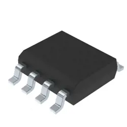
이미지는 참조용만
IS61WV25616BLL-10BLI
IC SRAM 4MBIT PARALLEL 48MINIBGA
- 제조업체
- Mfr.부분 #IS61WV25616BLL-10BLI
- 패키지 48-TFBGA
- 데이터시트 IS61WV25616BLL-10BLI DataSheet
- 재고 있음4509
100% 원래 &새로운
배송 준비 24 시간
365 일 보장
RFQ 및더 많은 할인
사양
| Package | Tray |
| ProductStatus | Active |
| MemoryType | Volatile |
| MemoryFormat | SRAM |
| Technology | SRAM - Asynchronous |
| MemorySize | 4Mb (256K x 16) |
| MemoryInterface | Parallel |
| WriteCycleTime-WordPage | 10ns |
| AccessTime | 10 ns |
| Voltage-Supply | 2.4V ~ 3.6V |
| OperatingTemperature | -40°C ~ 85°C (TA) |
| MountingType | Surface Mount |
| Package/Case | 48-TFBGA |
개요
Description
With a fast access time of 10 nanoseconds, this SRAM ensures high-speed data retrieval, ideal for cache memory and other performance-sensitive applications. The chip offers a simple interface for read and write operations, making it easy to integrate into various systems. It is available in a compact package, enhancing its suitability for space-constrained designs.
Overall, the IS61WV25616BLL-10BLI is an efficient choice for applications in telecommunications, networking, and consumer electronics where quick data processing and low power consumption are critical.
Features
1. Access Time: 10 ns, providing quick data retrieval.
2. Operating Voltage: Typically operates at 3.0V to 3.6V, suitable for various low-power applications.
3. Low Power Consumption: Designed for low active and standby power usage, enhancing energy efficiency.
4. Asynchronous Operation: Simplifies integration in systems needing fast response times.
5. Wide Operating Range: Supports a broad range of temperatures and operating conditions.
6. Data Retention: Maintains data integrity during power-down conditions.
7. Fast Write Cycle Times: Efficient write capabilities enhance performance for high-speed applications.
This SRAM is ideal for use in networking, telecommunications, and consumer electronics where speed and reliability are critical.
Package
Pinout
### Pin Functions:
- Address Pins (A0-A17): Used to select the memory location.
- Data Pins (DQ0-DQ15): Bi-directional data bus for reading from and writing to the memory.
- Control Pins:
- CLK: Clock input for synchronization.
- CKE: Clock enable for power management.
- CS: Chip select, enables the device for communication.
- RAS: Row address strobe for row selection.
- CAS: Column address strobe for column selection.
- WE: Write enable, for write operations.
- Baud Pins (BA0, BA1): Bank address pins for selecting the memory bank.
- VDD/VSS: Power supply and ground pins.
The device operates at a maximum clock frequency of 100 MHz, allowing for high-speed data access in various applications.
Manufacturer
Application
Equivalent
1. Micron MT48LC16M16A2P-75
2. Samsung K4S561632D-TC75
3. Hynix HY57V161620BTP-75
These alternatives offer similar specifications, such as data width and density, but always check for specific application compatibility before replacement.
배송
배송 방법We
DHL, FedEx, TNT, UPS 또는 선택한 다른 운송업체를 통해 글로벌 배송 서비스를 제공합니다.
배송 요금 참조 (DHL/FedEx):
DHL은: 배송 비용은 $25-$45 (0.5kg)에서 2-5 영업일의 추정적 배달 시간이 있습니다.
FedEx는: 배송 비용은 $25-$40 (0.5kg)에서 3-7 영업일의 추정적 배달 시간을 가지고 있습니다.
UPS는: 배송 비용은 $25-$45 (0.5kg)에서 3-7 영업일의 추정적 배달 시간을 가지고 있습니다.
TNT는: 배송 비용은 $25-$65 (0.5kg)에서 3-7 영업일의 추정적 배달 시간을 가지고 있습니다.
EMS는: 배송 비용은 $30-$50 (0.5kg)에서 7-15 영업일의 추정적 배달 시간을 제공합니다.
등록된 항공우편: 배송 비용은 $2-$4 (0.1kg), 예상 배달 시간 5-20 영업일.
지불
Payment Methods
지불 기간은 100% 사전 지불입니다.
현재, 우리는 아래 지불 방법만 받아들입니다.:
1. PayPal
2. 신용/직불 카드
3. 전선 전송
비슷한
-
![MX25L3233FM1I-08Q]() MX25L3233FM1I-08Q
Macronix
-
![MX29F400CBTI-70G]() MX29F400CBTI-70G
Macronix
-
![MX25V4035FZUI]() MX25V4035FZUI
Macronix
-
![MX25V2033FM1I]() MX25V2033FM1I
Macronix
-
![MX25V16066M2I02]() MX25V16066M2I02
Macronix
-
![MX30LF2G28AD-TI]() MX30LF2G28AD-TI
Macronix
-
![MX25R6435FBDIL0]() MX25R6435FBDIL0
Macronix
-
![MX25L25673GMI-08G]() MX25L25673GMI-08G
Macronix
-
![MX25U51279GXDR00]() MX25U51279GXDR00
Macronix
-
![MX25V1635FM2I]() MX25V1635FM2I
Macronix
-
![MX25L12833FZNI-10G]() MX25L12833FZNI-10..
Macronix
-
![MX29LV160DTTI-70G]() MX29LV160DTTI-70G
Macronix