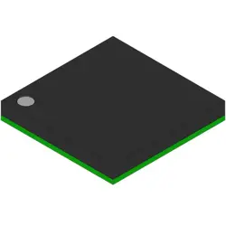
이미지는 참조용만
LFE2M35E-5FN484C
IC FPGA 303 I/O 484FBGA
- 제조업체
- Mfr.부분 #LFE2M35E-5FN484C
- 패키지 FPBGA-484
- 데이터시트 LFE2M35E-5FN484C DataSheet
- 재고 있음5186
100% 원래 &새로운
배송 준비 24 시간
365 일 보장
RFQ 및더 많은 할인
사양
| Package | Tray |
| Series | ECP2M |
| ProductStatus | Active |
| NumberofLABs/CLBs | 4250 |
| NumberofLogicElements/Cells | 34000 |
| TotalRAMBits | 2151424 |
| NumberofI/O | 303 |
| Voltage-Supply | 1.14V ~ 1.26V |
| MountingType | Surface Mount |
| OperatingTemperature | 0°C ~ 85°C (TJ) |
| Package/Case | 484-BBGA |
개요
Description
Key specifications include a 5V tolerance, 484-pin Fine Pitch Ball Grid Array (FBGA) package, and a maximum operating frequency of up to 500 MHz. It supports a variety of I/O standards, including LVDS and LVPECL, providing flexibility for interfacing with different components. The device includes built-in memory (Block RAM) and DSP slices, enhancing its capabilities for complex processing tasks.
The LFE2M35E is particularly valued for its cost-effectiveness and ease of use, with support from various development tools and design software, facilitating rapid prototyping and deployment in diverse applications.
Features
- Logic Elements: 35,000 LUTs (Look-Up Tables) for flexible logic implementation.
- I/O Pins: 484-ball Fine-Pitch BGA package with up to 32 I/O pins.
- Performance: Supports high-speed operation with up to 150 MHz performance.
- Embedded Memory: Includes up to 1.6 Mbits of embedded block RAM for efficient data storage.
- DSP Blocks: Features 36 DSP slices for digital signal processing tasks.
- Power Efficiency: Operates at low power, making it suitable for battery-operated devices.
- Configuration Options: Supports multiple configuration methods including JTAG and flash memory.
- Development Tools: Compatible with Lattice’s Diamond and Radiant development tools for design and simulation.
This FPGA is ideal for applications requiring a balance of performance, power efficiency, and configurability.
Package
Pinout
The primary functions of these pins include:
1. I/O Pins: Used for general input/output operations, supporting various standards and protocols.
2. Power Pins: Provide necessary power supply to the device.
3. Configuration Pins: Used for device configuration during power-up.
4. Clock Pins: Support clock signals for synchronous operations.
5. Ground Pins: Serve as ground connections for circuit stability.
This FPGA is designed for a range of applications, including communications, industrial automation, and consumer electronics, offering flexibility for custom logic implementation.
Manufacturer
Application
Equivalent
1. Xilinx Spartan-6 (e.g., XC6SLX25)
2. Intel MAX 10 (e.g., 10M50DAF484C8G)
3. Microchip IGLOO2 (e.g., AGLN250)
These alternatives may vary in features, I/O counts, and performance, so consider specific requirements for your application.
배송
배송 방법We
DHL, FedEx, TNT, UPS 또는 선택한 다른 운송업체를 통해 글로벌 배송 서비스를 제공합니다.
배송 요금 참조 (DHL/FedEx):
DHL은: 배송 비용은 $25-$45 (0.5kg)에서 2-5 영업일의 추정적 배달 시간이 있습니다.
FedEx는: 배송 비용은 $25-$40 (0.5kg)에서 3-7 영업일의 추정적 배달 시간을 가지고 있습니다.
UPS는: 배송 비용은 $25-$45 (0.5kg)에서 3-7 영업일의 추정적 배달 시간을 가지고 있습니다.
TNT는: 배송 비용은 $25-$65 (0.5kg)에서 3-7 영업일의 추정적 배달 시간을 가지고 있습니다.
EMS는: 배송 비용은 $30-$50 (0.5kg)에서 7-15 영업일의 추정적 배달 시간을 제공합니다.
등록된 항공우편: 배송 비용은 $2-$4 (0.1kg), 예상 배달 시간 5-20 영업일.
지불
Payment Methods
지불 기간은 100% 사전 지불입니다.
현재, 우리는 아래 지불 방법만 받아들입니다.:
1. PayPal
2. 신용/직불 카드
3. 전선 전송
비슷한
-
![MX25R8035FM1IL0]() MX25R8035FM1IL0
Macronix
-
![MX66U1G45GXDI00]() MX66U1G45GXDI00
Macronix
-
![MX25L8035EM2I-10G]() MX25L8035EM2I-10G
Macronix
-
![MX29GL512FHXFI-11G]() MX29GL512FHXFI-11..
Macronix
-
![MX25R1635FZUIH0]() MX25R1635FZUIH0
Macronix
-
![MX25L12833FM2I-10G]() MX25L12833FM2I-10..
Macronix
-
![MX25L12833FZ2I-10G]() MX25L12833FZ2I-10..
Macronix
-
![MX25L12833FZNI-10G]() MX25L12833FZNI-10..
Macronix
-
![MX25U25645GXDI00]() MX25U25645GXDI00
Macronix
-
![MX25L25645GXDI-08G]() MX25L25645GXDI-08..
Macronix
-
![MX29F040CTI-70G]() MX29F040CTI-70G
Macronix
-
![MX29LV640ETTI-70G]() MX29LV640ETTI-70G
Macronix