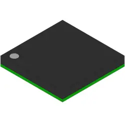
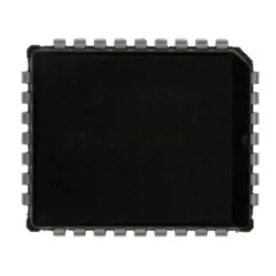
이미지는 참조용만
LFECP6E-5FN484C
IC FPGA 224 I/O 484FBGA
- 제조업체
- Mfr.부분 #LFECP6E-5FN484C
- 패키지 484-BBGA
- 데이터시트
- 재고 있음6884
100% 원래 &새로운
배송 준비 24 시간
365 일 보장
RFQ 및더 많은 할인
사양
| Package | Tray |
| Series | ECP |
| ProductStatus | Obsolete |
| NumberofLogicElements/Cells | 6100 |
| TotalRAMBits | 94208 |
| NumberofI/O | 224 |
| Voltage-Supply | 1.14V ~ 1.26V |
| MountingType | Surface Mount |
| OperatingTemperature | 0°C ~ 85°C (TJ) |
| Package/Case | 484-BBGA |
개요
Description
1. Architecture: It supports a range of logic elements, including LUTs, flip-flops, and dedicated DSP blocks, enabling complex logic implementations.
2. I/O Capabilities: The device has multiple I/O pins with flexible voltage standards, allowing it to interface with various peripherals.
3. Low Power Consumption: Designed for power-sensitive applications, it operates efficiently, making it suitable for battery-operated devices.
4. Applications: Common use cases include communications, industrial control, motor control, and video processing.
5. Development Tools: Lattice provides comprehensive development tools, such as Lattice Diamond and Radiant, facilitating design and debugging processes.
The LFECP6E-5FN484C is ideal for designers looking for a versatile, low-cost FPGA solution with a focus on power efficiency and performance.
Features
- Low Power Consumption: Designed for battery-operated and energy-efficient applications.
- High-Performance I/O: Supports various I/O standards, making it versatile for interfacing with different peripherals.
- Flexible Logic Architecture: Features include a combination of logic cells, DSP blocks, and memory resources, allowing for efficient implementation of complex algorithms.
- Built-in Clock Management: Equipped with clock management resources for better timing control and signal integrity.
- Development Support: Compatible with Lattice's design tools and development kits, facilitating easier design and prototyping.
- Small Form Factor: The FN484 package size is compact, suitable for space-constrained applications.
This FPGA is ideal for applications in communications, industrial automation, and consumer electronics where low power and high integration are essential.
Package
Pinout
The main functions of these pins include:
1. I/O Pins: Configurable for input, output, or bidirectional data transfer.
2. Power Supply Pins: Provide the necessary voltage levels for the FPGA operation.
3. Configuration Pins: Used for loading the configuration data into the FPGA at startup.
4. Clock Pins: Facilitate the input of clock signals for timing control within the FPGA.
5. Ground Pins: Ensure proper grounding for stability and performance.
The LFECP6E series is designed for applications requiring low power consumption, making it suitable for portable and battery-operated devices.
Manufacturer
Application
Equivalent
1. Xilinx Spartan-6 series (e.g., XC6SLX25)
2. Altera Cyclone IV series (e.g., EP4CE22)
3. Microsemi SmartFusion series
These alternatives may vary in logic density, features, and performance, so consider specific application requirements when choosing an equivalent.
배송
배송 방법We
DHL, FedEx, TNT, UPS 또는 선택한 다른 운송업체를 통해 글로벌 배송 서비스를 제공합니다.
배송 요금 참조 (DHL/FedEx):
DHL은: 배송 비용은 $25-$45 (0.5kg)에서 2-5 영업일의 추정적 배달 시간이 있습니다.
FedEx는: 배송 비용은 $25-$40 (0.5kg)에서 3-7 영업일의 추정적 배달 시간을 가지고 있습니다.
UPS는: 배송 비용은 $25-$45 (0.5kg)에서 3-7 영업일의 추정적 배달 시간을 가지고 있습니다.
TNT는: 배송 비용은 $25-$65 (0.5kg)에서 3-7 영업일의 추정적 배달 시간을 가지고 있습니다.
EMS는: 배송 비용은 $30-$50 (0.5kg)에서 7-15 영업일의 추정적 배달 시간을 제공합니다.
등록된 항공우편: 배송 비용은 $2-$4 (0.1kg), 예상 배달 시간 5-20 영업일.
지불
Payment Methods
지불 기간은 100% 사전 지불입니다.
현재, 우리는 아래 지불 방법만 받아들입니다.:
1. PayPal
2. 신용/직불 카드
3. 전선 전송
비슷한
-
![MX25V1635FZNI]() MX25V1635FZNI
Macronix
-
![MX25V1635FZNQ03]() MX25V1635FZNQ03
Macronix
-
![MX25V2033FM1I]() MX25V2033FM1I
Macronix
-
![MX25L8035EM2I-10G]() MX25L8035EM2I-10G
Macronix
-
![MX29GL512FHXFI-11G]() MX29GL512FHXFI-11..
Macronix
-
![MX25R1635FZUIH0]() MX25R1635FZUIH0
Macronix
-
![MX25L6433FM2I-08G]() MX25L6433FM2I-08G
Macronix
-
![MX29F040CQI-70G]() MX29F040CQI-70G
Macronix
-
![MX25L25645GXDI-08G]() MX25L25645GXDI-08..
Macronix
-
![MX30LF4G18AC-TI]() MX30LF4G18AC-TI
Macronix
-
![MX25L4006EM2I-12G]() MX25L4006EM2I-12G
Macronix
-
![MX25R4035FM1IL0]() MX25R4035FM1IL0
Macronix