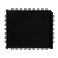
이미지는 참조용만
LTC1150CN8
IC OPAMP ZER-DRIFT 1CIRC 8DIP
- 제조업체
- Mfr.부분 #LTC1150CN8
- 패키지
- 데이터시트 LTC1150CN8 DataSheet
- 재고 있음111
100% 원래 &새로운
배송 준비 24 시간
365 일 보장
RFQ 및더 많은 할인
사양
| Part Status | Obsolete |
| Amplifier Type | Chopper (Zero-Drift) |
| Number of Circuits | 1 |
| Slew Rate | 3V/µs |
| Current - Input Bias | 10 pA |
| Voltage - Input Offset | 0.5 µV |
| Current - Supply | 800µA |
| Voltage - Supply Span (Min) | 4.75 V |
| Voltage - Supply Span (Max) | 32 V |
| Operating Temperature | 0°C ~ 70°C |
| Mounting Type | Through Hole |
| Package / Case | 8-DIP (0.300", 7.62mm) |
| Supplier Device Package | 8-PDIP |
| Base Product Number | LTC1150 |
| Gain Bandwidth Product | 2.5 MHz |
개요
Description
Key specifications include a low supply current, typically less than 1 mA, and a common-mode input range that extends to the negative supply rail, enhancing its versatility in various circuits. The LTC1150CN8 is commonly used in applications such as zero-crossing detectors, pulse-width modulation, and analog-to-digital converters.
The package type is a standard 8-lead PDIP (Plastic Dual In-line Package), facilitating easy integration into both prototype and production designs. Its combination of speed, precision, and low power consumption makes it an excellent choice for engineers looking to implement reliable comparison functions in their electronic designs.
Features
1. Fast Response: It offers a propagation delay of 25 ns and a slew rate of 30 V/µs, which makes it suitable for high-speed applications.
2. Low Power Consumption: The device operates with a supply voltage range from ±2 V to ±15 V and consumes low quiescent current, enhancing efficiency.
3. High Precision: It boasts a low input offset voltage of 0.5 mV maximum and a low input bias current, ensuring accurate signal comparisons.
4. Wide Common-Mode Range: The device supports a wide input common-mode voltage range, allowing it to function effectively with various signal levels.
5. Open-Collector Output: The output stage is an open-collector configuration, enabling easy interfacing with different voltage levels.
6. Hysteresis Control: It has the option for positive feedback, allowing users to implement hysteresis for improved noise immunity.
These features make the LTC1150CN8 ideal for applications in signal conditioning, voltage level detection, and analog-to-digital conversion systems.
Package
Pinout
1. Input Pins (IN+ and IN-): Two differential input pins for each comparator.
2. Output Pins (OUT): Two output pins corresponding to each comparator, providing the output signal.
3. V+ (Pin 8): Positive supply voltage pin.
4. GND (Pin 4): Ground reference pin.
5. Comp (Pin 6): Compensation pin for stability.
6. V- (Pin 1): Negative supply voltage pin.
The device is designed for low power operation and has a fast response time, making it suitable for applications requiring precise analog signal comparison.
Manufacturer
Application
Equivalent
배송
배송 방법We
DHL, FedEx, TNT, UPS 또는 선택한 다른 운송업체를 통해 글로벌 배송 서비스를 제공합니다.
배송 요금 참조 (DHL/FedEx):
DHL은: 배송 비용은 $25-$45 (0.5kg)에서 2-5 영업일의 추정적 배달 시간이 있습니다.
FedEx는: 배송 비용은 $25-$40 (0.5kg)에서 3-7 영업일의 추정적 배달 시간을 가지고 있습니다.
UPS는: 배송 비용은 $25-$45 (0.5kg)에서 3-7 영업일의 추정적 배달 시간을 가지고 있습니다.
TNT는: 배송 비용은 $25-$65 (0.5kg)에서 3-7 영업일의 추정적 배달 시간을 가지고 있습니다.
EMS는: 배송 비용은 $30-$50 (0.5kg)에서 7-15 영업일의 추정적 배달 시간을 제공합니다.
등록된 항공우편: 배송 비용은 $2-$4 (0.1kg), 예상 배달 시간 5-20 영업일.
지불
Payment Methods
지불 기간은 100% 사전 지불입니다.
현재, 우리는 아래 지불 방법만 받아들입니다.:
1. PayPal
2. 신용/직불 카드
3. 전선 전송
비슷한
-
![MX25L3233FZBI-08Q]() MX25L3233FZBI-08Q
Macronix
-
![MX25V5126FM1I]() MX25V5126FM1I
Macronix
-
![MX25V2033FM1I]() MX25V2033FM1I
Macronix
-
![MX30LF2G28AD-TI]() MX30LF2G28AD-TI
Macronix
-
![MX25R6435FBDIL0]() MX25R6435FBDIL0
Macronix
-
![MX25L25673GMI-08G]() MX25L25673GMI-08G
Macronix
-
![MX25U51279GXDR00]() MX25U51279GXDR00
Macronix
-
![MX25U6435FM2I-10G]() MX25U6435FM2I-10G
Macronix
-
![MX25L12833FM2I-10G]() MX25L12833FM2I-10..
Macronix
-
![MX25L12833FZ2I-10G]() MX25L12833FZ2I-10..
Macronix
-
![MX29F040CQI-70G]() MX29F040CQI-70G
Macronix
-
![MX29F800CBTI-70G]() MX29F800CBTI-70G
Macronix