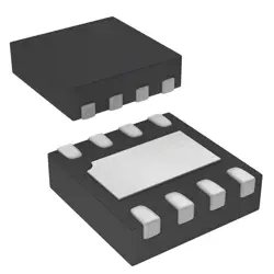
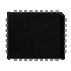
이미지는 참조용만
LTC6957HMS-2#PBF
IC CLK BUFFER DVR 1:2 12MSOP
- 제조업체
- Mfr.부분 #LTC6957HMS-2#PBF
- 패키지 12-TSSOP (0.118, 3.00mm Width)
- 데이터시트
- 재고 있음6116
100% 원래 &새로운
배송 준비 24 시간
365 일 보장
RFQ 및더 많은 할인
사양
| Supplier | Analog Devices Inc. |
| Package | Tube |
| ProductStatus | Active |
| Type | Fanout Buffer (Distribution) |
| NumberofCircuits | 1 |
| Ratio-Input:Output | 1:2 |
| Differential-Input:Output | Yes/Yes |
| Input | CML, CMOS, LVDS, LVPECL |
| Output | LVDS |
| Frequency-Max | 300 MHz |
| Voltage-Supply | 3.15V ~ 3.45V |
| OperatingTemperature | -40°C ~ 125°C |
| MountingType | Surface Mount |
| Package/Case | 12-TSSOP (0.118, 3.00mm Width) |
개요
Description
Key points
- 2-output variant (LTC6957 family): HMS indicates the HSMSOP-16 package; -2 denotes two outputs.
- Low jitter / low skew clock distribution suitable for FPGA, SERDES, processors, telecom, and precision ADC/DAC timing.
- Typically operates from a standard supply (e.g., 3.3 V) and accepts a reference clock input; outputs can be configured for compatible signaling standards (per datasheet).
- -PBF signifies RoHS-compliant, lead-free packaging.
What to do next
- Check the LTC6957 datasheet for exact electrical specs, input/output formats, drive strength, power-down features, and recommended app circuits.
- Review the pinout and typical use-cases to ensure compatibility with your reference clock and target devices.
Features
- Dual low-jitter clock outputs (differential) with selectable output formats (LVPECL/LVDS/CMOS)
- Programmable frequency synthesis via an internal/N-divider scheme to derive output frequencies from a reference
- Jitter-cleaning PLL with good phase noise performance
- Independent enable/disable and robust holdover options
- Wide single-supply operation (compatible with common rails around 2.5–3.3 V)
- Industrial temperature range (typical -40°C to 125°C)
- Low power consumption for clock distribution applications
- Small RoHS-compliant package (HMS) with lead-free (#PBF) variant
- Serial or simple control interface for configuring dividers/dividers/modes (often SPI-like)
For exact electrical specs, timing details, and package pinout, please refer to the official LTC6957HMS-2#PBF datasheet.
Package
Pinout
- Function: High-performance jitter-cleaning clock generator/PLL with dual outputs; provides two synchronized clock signals derived from a reference, with selectable division/multiplication for clock distribution (used for precise timing in high-speed interfaces).
Manufacturer
Application
- High-speed clock distribution to FPGAs/ASICs/DSPs
- Clocking SERDES interfaces (PCIe, SATA, JESD204B, other high-speed links)
- Telecom and data‑communication equipment and backplanes
- RF/IF systems and ADC/DAC sampling clocks
- Test and measurement instrumentation and other timing-critical systems
배송
배송 방법We
DHL, FedEx, TNT, UPS 또는 선택한 다른 운송업체를 통해 글로벌 배송 서비스를 제공합니다.
배송 요금 참조 (DHL/FedEx):
DHL은: 배송 비용은 $25-$45 (0.5kg)에서 2-5 영업일의 추정적 배달 시간이 있습니다.
FedEx는: 배송 비용은 $25-$40 (0.5kg)에서 3-7 영업일의 추정적 배달 시간을 가지고 있습니다.
UPS는: 배송 비용은 $25-$45 (0.5kg)에서 3-7 영업일의 추정적 배달 시간을 가지고 있습니다.
TNT는: 배송 비용은 $25-$65 (0.5kg)에서 3-7 영업일의 추정적 배달 시간을 가지고 있습니다.
EMS는: 배송 비용은 $30-$50 (0.5kg)에서 7-15 영업일의 추정적 배달 시간을 제공합니다.
등록된 항공우편: 배송 비용은 $2-$4 (0.1kg), 예상 배달 시간 5-20 영업일.
지불
Payment Methods
지불 기간은 100% 사전 지불입니다.
현재, 우리는 아래 지불 방법만 받아들입니다.:
1. PayPal
2. 신용/직불 카드
3. 전선 전송
비슷한
-
![MX25V2033FM1I]() MX25V2033FM1I
Macronix
-
![MX25V16066M2I02]() MX25V16066M2I02
Macronix
-
![MX25R6435FBDIL0]() MX25R6435FBDIL0
Macronix
-
![MX25U25643GZNI00]() MX25U25643GZNI00
Macronix
-
![MX25U3232FZBI02]() MX25U3232FZBI02
Macronix
-
![MX25U6435FM2I-10G]() MX25U6435FM2I-10G
Macronix
-
![MX25L12833FZNI-10G]() MX25L12833FZNI-10..
Macronix
-
![MX25L12835FZ2I-10G]() MX25L12835FZ2I-10..
Macronix
-
![MX29LV160DTTI-70G]() MX29LV160DTTI-70G
Macronix
-
![MX29F040CQI-70G]() MX29F040CQI-70G
Macronix
-
![MX29LV640ETTI-70G]() MX29LV640ETTI-70G
Macronix
-
![MX25L25735FMI-10G]() MX25L25735FMI-10G
Macronix