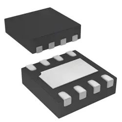
이미지는 참조용만
MAX1673ESA+
IC REG CHARGE PUMP ADJ 8SOIC
- 제조업체
- Mfr.부분 #MAX1673ESA+
- 패키지 SOP8
- 데이터시트
- 재고 있음519
100% 원래 &새로운
배송 준비 24 시간
365 일 보장
RFQ 및더 많은 할인
사양
| Package | Tube,Tube |
| ProductStatus | Obsolete |
| Function | Step-Down |
| OutputConfiguration | Negative |
| Topology | Charge Pump |
| OutputType | Adjustable |
| NumberofOutputs | 1 |
| Voltage-Input(Min) | 2V |
| Voltage-Input(Max) | 5.5V |
| Voltage-Output(Min/Fixed) | -1.5V |
| Voltage-Output(Max) | -5.5V |
| Current-Output | 125mA |
| Frequency-Switching | 350kHz |
| SynchronousRectifier | No |
| OperatingTemperature | -40°C ~ 85°C (TA) |
| MountingType | Surface Mount |
| Package/Case | 8-SOIC (0.154, 3.90mm Width) |
개요
Description
The MAX1673ESA+ employs a built-in PWM control scheme to enhance efficiency, minimizing power loss during operation. It incorporates features such as a shutdown mode to conserve battery life and a soft-start function to reduce inrush current. The device is available in a 10-pin MSOP package, making it suitable for compact applications. Overall, the MAX1673ESA+ is ideal for portable electronics, IoT devices, and other applications requiring reliable power conversion from low-voltage sources.
Features
1. Output Voltage: Adjustable output voltage range from 1.3V to 5.5V.
2. Input Voltage Range: Operates from 2.5V to 6V.
3. High Efficiency: Up to 95% efficiency, minimizing power loss.
4. Low Dropout Voltage: Typically 200mV at full load, allowing operation with low input voltages.
5. Load Regulation: Excellent load regulation characteristics.
6. Quiescent Current: Low quiescent current (typically 20µA) for battery-operated devices.
7. Thermal Shutdown: Integrated thermal protection to prevent overheating.
8. Overcurrent Protection: Safeguards against output overcurrent conditions.
9. Package: Available in a space-saving SOIC-8 package.
These features make the MAX1673ESA+ suitable for various applications, including portable devices, communication equipment, and battery-powered systems.
Package
Pinout
The pin configuration includes the following functions:
1. VIN (Pin 1): Input voltage.
2. GND (Pin 2): Ground reference.
3. SW (Pin 3): Switch node for the inductor.
4. VOUT (Pin 4): Output voltage.
5. COMP (Pin 5): Compensation pin for stability.
6. RSET (Pin 6): Resistor for setting the output voltage.
7. EN (Pin 7): Enable pin to turn the device on/off.
8. FB (Pin 8): Feedback pin for voltage regulation.
This device is widely used in applications that require efficient voltage conversion with minimal external components.
Manufacturer
Application
Equivalent
배송
배송 방법We
DHL, FedEx, TNT, UPS 또는 선택한 다른 운송업체를 통해 글로벌 배송 서비스를 제공합니다.
배송 요금 참조 (DHL/FedEx):
DHL은: 배송 비용은 $25-$45 (0.5kg)에서 2-5 영업일의 추정적 배달 시간이 있습니다.
FedEx는: 배송 비용은 $25-$40 (0.5kg)에서 3-7 영업일의 추정적 배달 시간을 가지고 있습니다.
UPS는: 배송 비용은 $25-$45 (0.5kg)에서 3-7 영업일의 추정적 배달 시간을 가지고 있습니다.
TNT는: 배송 비용은 $25-$65 (0.5kg)에서 3-7 영업일의 추정적 배달 시간을 가지고 있습니다.
EMS는: 배송 비용은 $30-$50 (0.5kg)에서 7-15 영업일의 추정적 배달 시간을 제공합니다.
등록된 항공우편: 배송 비용은 $2-$4 (0.1kg), 예상 배달 시간 5-20 영업일.
지불
Payment Methods
지불 기간은 100% 사전 지불입니다.
현재, 우리는 아래 지불 방법만 받아들입니다.:
1. PayPal
2. 신용/직불 카드
3. 전선 전송
비슷한
-
![MX25V1635FZNQ03]() MX25V1635FZNQ03
Macronix
-
![MX29F400CBTI-70G]() MX29F400CBTI-70G
Macronix
-
![MX25V4035FZUI]() MX25V4035FZUI
Macronix
-
![MX25R3235FZNIL0]() MX25R3235FZNIL0
Macronix
-
![MX25L8035EM2I-10G]() MX25L8035EM2I-10G
Macronix
-
![MX25R6435FBDIL0]() MX25R6435FBDIL0
Macronix
-
![MX25U25643GZNI00]() MX25U25643GZNI00
Macronix
-
![MX25R1635FZUIH0]() MX25R1635FZUIH0
Macronix
-
![MX25V1635FM2I]() MX25V1635FM2I
Macronix
-
![MX25U3232FZBI02]() MX25U3232FZBI02
Macronix
-
![MX25L6433FM2I-08G]() MX25L6433FM2I-08G
Macronix
-
![MX25L12833FZ2I-10G]() MX25L12833FZ2I-10..
Macronix