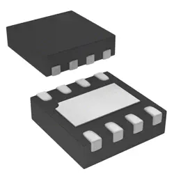
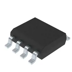
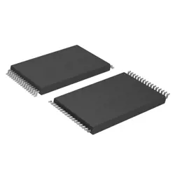
이미지는 참조용만
MAX40100ANT+T
IC OPAMP ZERO-DRIFT 1 CIRC 6WLP
- 제조업체
- Mfr.부분 #MAX40100ANT+T
- 패키지 WLP-6
- 데이터시트
- 재고 있음6599
100% 원래 &새로운
배송 준비 24 시간
365 일 보장
RFQ 및더 많은 할인
사양
| Package | Tape & Reel (TR),Cut Tape (CT) |
| ProductStatus | Active |
| AmplifierType | Zero-Drift |
| NumberofCircuits | 1 |
| OutputType | Rail-to-Rail |
| SlewRate | 0.7V/µs |
| GainBandwidthProduct | 1.5 MHz |
| Current-InputBias | 80 pA |
| Current-Supply | 66µA |
| Voltage-SupplySpan(Min) | 1.6 V |
| Voltage-SupplySpan(Max) | 5.5 V |
| OperatingTemperature | -40°C ~ 125°C |
| MountingType | Surface Mount |
| Package/Case | 6-XFBGA, WLPBGA |
개요
Description
Key specifications include a gain bandwidth product of 1.8 MHz, a low input offset voltage of 200 µV, and a low noise density of 11 nV/√Hz. This amplifier operates from a single supply voltage, ranging from 2.7V to 5.5V, which enhances its versatility in battery-powered applications.
The small SOT23-5 package allows for easy integration into compact designs. Its fast response time and high slew rate make it ideal for applications requiring rapid signal processing. Overall, the MAX40100ANT+T combines performance and efficiency, making it a popular choice among designers for precision analog signal applications.
Features
1. Supply Voltage Range: Operates from 2.7V to 5.5V.
2. High Bandwidth: Gain bandwidth product of 80 MHz, enabling fast signal processing.
3. Low Input Offset Voltage: Typically 0.2 mV, ensuring high accuracy.
4. Low Noise: Input voltage noise density of 16 nV/√Hz at 1 kHz, supporting clean signal amplification.
5. Rail-to-Rail Output: Allows the output to swing to within 50 mV of the power supply rails, maximizing output range.
6. Low Power Consumption: Quiescent current of 1.3 mA, ideal for battery-operated devices.
7. High Slew Rate: 70 V/µs, facilitating rapid signal changes without distortion.
8. Temperature Range: Operates from -40°C to +125°C, suitable for a variety of environments.
These features make the MAX40100ANT+T suitable for applications in data acquisition, sensor signal conditioning, and medical devices.
Package
Pinout
Pin Functions:
1. OUT (Pin 1): Output of the op-amp.
2. IN+ (Pin 2): Non-inverting input.
3. IN- (Pin 3): Inverting input.
4. V- (Pin 4): Negative power supply pin.
5. V+ (Pin 5): Positive power supply pin.
This device is designed for low power consumption and high-speed operation, making it suitable for various applications such as sensor signal conditioning and active filtering.
Manufacturer
Application
Equivalent
배송
배송 방법We
DHL, FedEx, TNT, UPS 또는 선택한 다른 운송업체를 통해 글로벌 배송 서비스를 제공합니다.
배송 요금 참조 (DHL/FedEx):
DHL은: 배송 비용은 $25-$45 (0.5kg)에서 2-5 영업일의 추정적 배달 시간이 있습니다.
FedEx는: 배송 비용은 $25-$40 (0.5kg)에서 3-7 영업일의 추정적 배달 시간을 가지고 있습니다.
UPS는: 배송 비용은 $25-$45 (0.5kg)에서 3-7 영업일의 추정적 배달 시간을 가지고 있습니다.
TNT는: 배송 비용은 $25-$65 (0.5kg)에서 3-7 영업일의 추정적 배달 시간을 가지고 있습니다.
EMS는: 배송 비용은 $30-$50 (0.5kg)에서 7-15 영업일의 추정적 배달 시간을 제공합니다.
등록된 항공우편: 배송 비용은 $2-$4 (0.1kg), 예상 배달 시간 5-20 영업일.
지불
Payment Methods
지불 기간은 100% 사전 지불입니다.
현재, 우리는 아래 지불 방법만 받아들입니다.:
1. PayPal
2. 신용/직불 카드
3. 전선 전송
비슷한
-
![MX25V1635FZNQ03]() MX25V1635FZNQ03
Macronix
-
![MX25V2033FM1I]() MX25V2033FM1I
Macronix
-
![MX25U51279GXDR00]() MX25U51279GXDR00
Macronix
-
![MX25L2006EM1I-12G]() MX25L2006EM1I-12G
Macronix
-
![MX25R1635FZUIH0]() MX25R1635FZUIH0
Macronix
-
![MX25V1635FM2I]() MX25V1635FM2I
Macronix
-
![MX25L6433FM2I-08G]() MX25L6433FM2I-08G
Macronix
-
![MX25L12833FZ2I-10G]() MX25L12833FZ2I-10..
Macronix
-
![MX25U25645GXDI00]() MX25U25645GXDI00
Macronix
-
![MX29F040CTI-70G]() MX29F040CTI-70G
Macronix
-
![MX30LF4G18AC-TI]() MX30LF4G18AC-TI
Macronix
-
![MX25U51245GZ4I00]() MX25U51245GZ4I00
Macronix