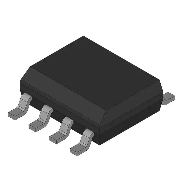
이미지는 참조용만
MAX680ESA+T
IC REG CHARGE PUMP 2VIN 8SOIC
- 제조업체
- Mfr.부분 #MAX680ESA+T
- 패키지 SOIC-Narrow-8
- 데이터시트
- 재고 있음4101
100% 원래 &새로운
배송 준비 24 시간
365 일 보장
RFQ 및더 많은 할인
사양
| Package | Tape & Reel (TR),Bulk |
| ProductStatus | Obsolete |
| Function | Ratiometric |
| OutputConfiguration | Positive and Negative (Dual Rail) |
| Topology | Charge Pump |
| OutputType | Fixed |
| NumberofOutputs | 2 |
| Voltage-Input(Min) | 2V |
| Voltage-Input(Max) | 6V |
| Voltage-Output(Min/Fixed) | ±2Vin |
| Current-Output | 10mA |
| Frequency-Switching | 8kHz |
| SynchronousRectifier | No |
| OperatingTemperature | -40°C ~ 85°C (TA) |
| MountingType | Surface Mount |
| Package/Case | 8-SOIC (0.154, 3.90mm Width) |
개요
Description
Key features of the MAX680ESA+T include its low supply current and the ability to deliver a regulated negative output voltage without requiring inductors, which simplifies the design and reduces the size and cost of the end product. It operates over a wide input voltage range and is capable of providing a consistent output even with varying input conditions.
The MAX680ESA+T comes in an 8-pin SOIC package, making it suitable for compact applications. It is designed for ease of use with few external components required, improving design efficiency. Its typical applications include dual power supply systems, operational amplifiers, and data acquisition systems.
Features
1. Input Voltage Range: Operates with an input voltage range of 2V to 5.5V.
2. Output Voltage: Doubles the input voltage to provide an output of up to 10V.
3. Low Quiescent Current: Features a low quiescent current, typically 110µA, which enhances battery life in portable applications.
4. Shutdown Mode: Includes a shutdown mode, reducing current consumption to a mere 1µA.
5. Low Supply Current: Efficient with low supply and operating current.
6. Small Package: Available in an 8-pin SOIC package, making it suitable for space-constrained designs.
7. High Efficiency: Delivers high efficiency at low to moderate load currents.
8. Built-in Oscillator: Contains an internal oscillator with a fixed frequency.
9. Temperature Range: Operates over a wide temperature range suitable for industrial applications.
These features make the MAX680ESA+T ideal for applications requiring a compact, low-power, and efficient solution for generating higher voltages from a single supply.
Package
Pinout
The device comes in an 8-pin SOIC (Small Outline Integrated Circuit) package. The functions of the pins are as follows:
1. V+: Positive supply voltage input.
2. GND: Ground reference for the device.
3. CAP+: Positive terminal for the charge pump capacitor.
4. CAP-: Negative terminal for the charge pump capacitor.
5. OUT: Inverted negative voltage output.
6. LV: Logic input to select low-voltage operation.
7. SHDN: Shutdown control, active low to disable the device and reduce power consumption.
8. NC: No connection, this pin is not internally connected and can be left unconnected.
These pins facilitate the basic operation of inverting the input voltage with minimal external components.
Manufacturer
Application
Equivalent
배송
배송 방법We
DHL, FedEx, TNT, UPS 또는 선택한 다른 운송업체를 통해 글로벌 배송 서비스를 제공합니다.
배송 요금 참조 (DHL/FedEx):
DHL은: 배송 비용은 $25-$45 (0.5kg)에서 2-5 영업일의 추정적 배달 시간이 있습니다.
FedEx는: 배송 비용은 $25-$40 (0.5kg)에서 3-7 영업일의 추정적 배달 시간을 가지고 있습니다.
UPS는: 배송 비용은 $25-$45 (0.5kg)에서 3-7 영업일의 추정적 배달 시간을 가지고 있습니다.
TNT는: 배송 비용은 $25-$65 (0.5kg)에서 3-7 영업일의 추정적 배달 시간을 가지고 있습니다.
EMS는: 배송 비용은 $30-$50 (0.5kg)에서 7-15 영업일의 추정적 배달 시간을 제공합니다.
등록된 항공우편: 배송 비용은 $2-$4 (0.1kg), 예상 배달 시간 5-20 영업일.
지불
Payment Methods
지불 기간은 100% 사전 지불입니다.
현재, 우리는 아래 지불 방법만 받아들입니다.:
1. PayPal
2. 신용/직불 카드
3. 전선 전송
비슷한
-
![MX25L3233FZBI-08Q]() MX25L3233FZBI-08Q
Macronix
-
![MX25R1635FZUIH0]() MX25R1635FZUIH0
Macronix
-
![MX25V1635FM2I]() MX25V1635FM2I
Macronix
-
![MX25L12833FM2I-10G]() MX25L12833FM2I-10..
Macronix
-
![MX25L12833FZ2I-10G]() MX25L12833FZ2I-10..
Macronix
-
![MX25U25645GXDI00]() MX25U25645GXDI00
Macronix
-
![MX29LV160DTTI-70G]() MX29LV160DTTI-70G
Macronix
-
![MX29F040CTI-70G]() MX29F040CTI-70G
Macronix
-
![MX25L1006EMI-10G]() MX25L1006EMI-10G
Macronix
-
![MX25L4006EM2I-12G]() MX25L4006EM2I-12G
Macronix
-
![MX25V8035FM2I]() MX25V8035FM2I
Macronix
-
![MX25U3232FM2I02]() MX25U3232FM2I02
Macronix