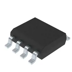
이미지는 참조용만
MT48LC8M16A2P-75:G
IC DRAM 128MBIT PAR 54TSOP II
- 제조업체
- Mfr.부분 #MT48LC8M16A2P-75:G
- 패키지
- 데이터시트
- 재고 있음3333
100% 원래 &새로운
배송 준비 24 시간
365 일 보장
RFQ 및더 많은 할인
사양
| Part Status | Obsolete |
| Base Product Number | MT48LC8M16A2 |
| DigiKey Programmable | Not Verified |
| Memory Type | Volatile |
| Memory Format | DRAM |
| Technology | SDRAM |
| Memory Size | 128Mbit |
| Memory Organization | 8M x 16 |
| Memory Interface | Parallel |
| Clock Frequency | 133 MHz |
| Write Cycle Time - Word, Page | 15ns |
| Voltage - Supply | 3V ~ 3.6V |
| Operating Temperature | 0°C ~ 70°C (TA) |
| Mounting Type | Surface Mount |
| Package | 54-TSOP (0.400", 10.16mm Width) |
| Supplier Device Package | 54-TSOP II |
| Packaging | Tray |
| Access Time | 5.4 ns |
개요
Description
Key features include:
- Interface: It uses a synchronous interface, allowing for high-speed data transfers.
- Voltage: Operates typically at 2.5V, which contributes to lower power consumption.
- Package: Available in a compact 54-pin TSOP II package for efficient space utilization on circuit boards.
- Applications: Commonly used in consumer electronics, telecommunications, and computing devices, particularly where moderate-speed memory is sufficient.
This component is part of Micron's extensive line of memory solutions, designed to meet the growing demand for efficient and high-performance memory in modern electronic devices.
Features
1. Type: It is a DDR2 (Double Data Rate 2) synchronous dynamic random-access memory (SDRAM).
2. Organization: The chip has a x16 I/O configuration, allowing it to transfer data in 16-bit wide chunks.
3. Speed: It operates at a clock speed of 400 MT/s (megatransfers per second) with a data rate of 800 Mbps.
4. Voltage: The operating voltage is 1.8V, making it more power-efficient compared to earlier generations.
5. Package: It comes in a 54-ball FBGA (Fine Ball Grid Array) package, suitable for compact designs.
6. Refresh: The chip supports a refresh rate that complies with JEDEC standards.
7. Applications: It's commonly used in consumer electronics, networking, and various computing applications.
This memory is designed for high performance, low power consumption, and reliability in a variety of applications.
Package
Pinout
The key functions of the pins include:
- Data Pins (DQ0-DQ15): Used for data input/output.
- Address Pins (A0-A11): Used to select the memory address.
- Control Pins:
- CLK: Clock input for synchronous operation.
- CS: Chip select, enables the device.
- RAS: Row address strobe, used for row access.
- CAS: Column address strobe, used for column access.
- WE: Write enable, controls write operations.
- Power Supply Pins: Vdd and Vss for power connections.
- Other Pins:
- CKE: Clock enable, for power management.
- ODT: On-die termination.
This memory chip is typically used in various applications including mobile devices and consumer electronics.
Manufacturer
Application
Equivalent
1. Hynix HY5DU121622BFP-D43
2. Samsung K4S641632F-UL75
3. Nanya NT5CB256M16DP-75
4. Winbond W631GG6KB-75
Ensure compatibility based on specifications and application requirements before substitution.
배송
배송 방법We
DHL, FedEx, TNT, UPS 또는 선택한 다른 운송업체를 통해 글로벌 배송 서비스를 제공합니다.
배송 요금 참조 (DHL/FedEx):
DHL은: 배송 비용은 $25-$45 (0.5kg)에서 2-5 영업일의 추정적 배달 시간이 있습니다.
FedEx는: 배송 비용은 $25-$40 (0.5kg)에서 3-7 영업일의 추정적 배달 시간을 가지고 있습니다.
UPS는: 배송 비용은 $25-$45 (0.5kg)에서 3-7 영업일의 추정적 배달 시간을 가지고 있습니다.
TNT는: 배송 비용은 $25-$65 (0.5kg)에서 3-7 영업일의 추정적 배달 시간을 가지고 있습니다.
EMS는: 배송 비용은 $30-$50 (0.5kg)에서 7-15 영업일의 추정적 배달 시간을 제공합니다.
등록된 항공우편: 배송 비용은 $2-$4 (0.1kg), 예상 배달 시간 5-20 영업일.
지불
Payment Methods
지불 기간은 100% 사전 지불입니다.
현재, 우리는 아래 지불 방법만 받아들입니다.:
1. PayPal
2. 신용/직불 카드
3. 전선 전송
비슷한
-
![MX25R8035FM1IL0]() MX25R8035FM1IL0
Macronix
-
![MX25V1635FZNI]() MX25V1635FZNI
Macronix
-
![MX25V4035FZUI]() MX25V4035FZUI
Macronix
-
![MX25R3235FZNIL0]() MX25R3235FZNIL0
Macronix
-
![MX25V16066M2I02]() MX25V16066M2I02
Macronix
-
![MX25R6435FBDIL0]() MX25R6435FBDIL0
Macronix
-
![MX25U25643GZNI00]() MX25U25643GZNI00
Macronix
-
![MX25L2006EM1I-12G]() MX25L2006EM1I-12G
Macronix
-
![MX25V1635FM2I]() MX25V1635FM2I
Macronix
-
![MX25U6435FM2I-10G]() MX25U6435FM2I-10G
Macronix
-
![MX25U25645GXDI00]() MX25U25645GXDI00
Macronix
-
![MX29LV160DTTI-70G]() MX29LV160DTTI-70G
Macronix