
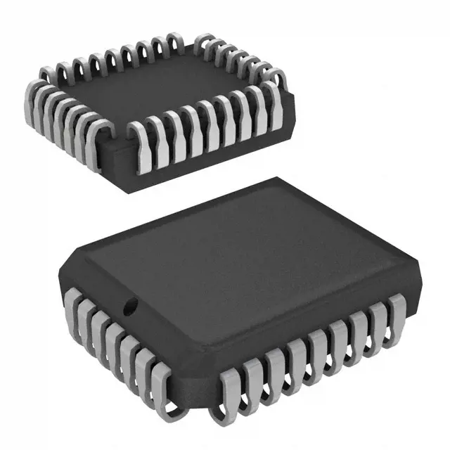
이미지는 참조용만
MX29LV040CQI-70G
IC FLASH 4MBIT PARALLEL 32PLCC
- 제조업체
- Mfr.부분 #MX29LV040CQI-70G
- 패키지
- 데이터시트
- 재고 있음4538
100% 원래 &새로운
배송 준비 24 시간
365 일 보장
RFQ 및더 많은 할인
사양
| Series | MX29LV |
| Part Status | Obsolete |
| Base Product Number | MX29LV040 |
| DigiKey Programmable | Not Verified |
| Memory Type | Non-Volatile |
| Memory Format | FLASH |
| Technology | FLASH - NOR |
| Memory Size | 4Mbit |
| Memory Organization | 512K x 8 |
| Memory Interface | Parallel |
| Write Cycle Time - Word, Page | 70ns |
| Voltage - Supply | 2.7V ~ 3.6V |
| Operating Temperature | -40°C ~ 85°C (TA) |
| Mounting Type | Surface Mount |
| Package | 32-LCC (J-Lead) |
| Supplier Device Package | 32-PLCC (11.43x14.05) |
| Packaging | Tray |
| Access Time | 70 ns |
개요
Description
This chip utilizes a standard 32-pin TSOP (Thin Small Outline Package) and supports both parallel and serial programming interfaces. It has a wide voltage range (typically 3V to 3.6V), enabling compatibility with various devices. The MX29LV040CQI-70G supports multiple read, erase, and program cycles, ensuring reliability and efficiency in data management.
Key features include fast read speeds, low power consumption, and the ability to perform sector or bulk erase operations. With its robust performance and reliability, the MX29LV040CQI-70G is ideal for applications in telecommunications, automotive, and industrial control systems.
Features
1. Technology: Uses CMOS technology for low power consumption.
2. Interface: Provides an 8-bit parallel I/O interface for data transfer.
3. Access Speed: Offers a maximum access time of 70 ns.
4. Programming Voltage: Operates at 3.0V to 3.6V for read and programming, ensuring compatibility with low-voltage systems.
5. Erase Capability: Supports sector erase and chip erase functions, with a typical erase time of 0.5 seconds per sector.
6. Endurance: Designed for a minimum of 100,000 program/erase cycles per sector.
7. Data Retention: Ensures data retention of over 20 years.
8. Package: Available in a 32-pin SOP (Small Outline Package) for space-efficient design.
These features make the MX29LV040CQI-70G suitable for applications in consumer electronics, telecommunications, and automotive systems.
Package
Pinout
Pin Functionality:
1. Address Pins (A0-A18): Used for addressing the memory locations.
2. Data Pins (DQ0-DQ7): 8-bit data input/output.
3. Chip Enable (CE): Activates the memory chip.
4. Output Enable (OE): Enables data output.
5. Write Enable (WE): Controls write operations.
6. Reset (RESET): Resets the internal state.
7. Common Ground (VSS): Ground reference.
8. Power Supply (VCC): Positive power supply for operation.
9. RMV (Ready/Busy): Indicates the status of read/write operations.
This device operates at a maximum access time of 70 ns and supports multiple read and write cycles, making it suitable for various applications in embedded systems.
Manufacturer
Application
Equivalent
1. Am29F040B - AMD
2. W29C040 - Winbond
3. S29GL040A - Spansion
4. AT49F040 - Atmel
These alternatives feature similar specifications, such as data width and access times. Always check specific compatibility for your application.
배송
배송 방법We
DHL, FedEx, TNT, UPS 또는 선택한 다른 운송업체를 통해 글로벌 배송 서비스를 제공합니다.
배송 요금 참조 (DHL/FedEx):
DHL은: 배송 비용은 $25-$45 (0.5kg)에서 2-5 영업일의 추정적 배달 시간이 있습니다.
FedEx는: 배송 비용은 $25-$40 (0.5kg)에서 3-7 영업일의 추정적 배달 시간을 가지고 있습니다.
UPS는: 배송 비용은 $25-$45 (0.5kg)에서 3-7 영업일의 추정적 배달 시간을 가지고 있습니다.
TNT는: 배송 비용은 $25-$65 (0.5kg)에서 3-7 영업일의 추정적 배달 시간을 가지고 있습니다.
EMS는: 배송 비용은 $30-$50 (0.5kg)에서 7-15 영업일의 추정적 배달 시간을 제공합니다.
등록된 항공우편: 배송 비용은 $2-$4 (0.1kg), 예상 배달 시간 5-20 영업일.
지불
Payment Methods
지불 기간은 100% 사전 지불입니다.
현재, 우리는 아래 지불 방법만 받아들입니다.:
1. PayPal
2. 신용/직불 카드
3. 전선 전송
비슷한
-
![MX25L3233FZBI-08Q]() MX25L3233FZBI-08Q
MX25L3233FZBI-08Q
Macronix
-
![MX25V1635FZNQ03]() MX25V1635FZNQ03
MX25V1635FZNQ03
Macronix
-
![MX25V5126FM1I]() MX25V5126FM1I
MX25V5126FM1I
Macronix
-
![MX25V16066M2I02]() MX25V16066M2I02
MX25V16066M2I02
Macronix
-
![MX25L25673GMI-08G]() MX25L25673GMI-08G
MX25L25673GMI-08G
Macronix
-
![MX29GL512FHXFI-11G]() MX29GL512FHXFI-11..
MX29GL512FHXFI-11..
Macronix
-
![MX25U3232FZBI02]() MX25U3232FZBI02
MX25U3232FZBI02
Macronix
-
![MX25L12833FM2I-10G]() MX25L12833FM2I-10..
MX25L12833FM2I-10..
Macronix
-
![MX25U25645GXDI00]() MX25U25645GXDI00
MX25U25645GXDI00
Macronix
-
![MX25L12835FZ2I-10G]() MX25L12835FZ2I-10..
MX25L12835FZ2I-10..
Macronix
-
![MX29F040CTI-70G]() MX29F040CTI-70G
MX29F040CTI-70G
Macronix
-
![MX29F800CBTI-70G]() MX29F800CBTI-70G
MX29F800CBTI-70G
Macronix







