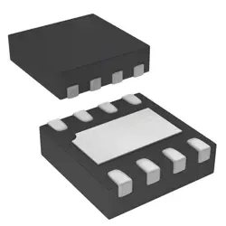
이미지는 참조용만
NSVRB751S40T1G
DIODE SCHOTTKY 30V 30MA SOD523
- 제조업체
- Mfr.부분 #NSVRB751S40T1G
- 패키지
- 데이터시트
- 재고 있음6318
100% 원래 &새로운
배송 준비 24 시간
365 일 보장
RFQ 및더 많은 할인
사양
| Part Status | Active |
| Technology | Schottky |
| Voltage - DC Reverse (Vr) (Max) | 30 V |
| Current - Average Rectified (Io) | 30mA |
| Voltage - Forward (Vf) (Max) @ If | 370 mV @ 1 mA |
| Speed | Small Signal =< 200mA (Io), Any Speed |
| Current - Reverse Leakage @ Vr | 500 nA @ 30 V |
| Capacitance @ Vr, F | 2.5pF @ 1V, 1MHz |
| Mounting Type | Surface Mount |
| Package / Case | SC-79, SOD-523 |
| Supplier Device Package | SOD-523 |
| Operating Temperature - Junction | -55°C ~ 150°C |
| Base Product Number | NSVRB751 |
| Grade | Automotive |
| Qualification | AEC-Q101 |
개요
Description
Key specifications typically include a maximum drain-source voltage (V_DS), a specified continuous drain current (I_D), and a low gate threshold voltage (V_GS(th)). The NSVRB751S40T1G is encapsulated in a compact surface-mount package, facilitating easy integration into circuit boards.
Overall, its robust performance characteristics make it a reliable choice for engineers and designers looking to implement efficient and effective electronic solutions.
Features
1. Voltage Rating: 40V maximum drain-source voltage (V_DS).
2. Current Rating: Capable of handling continuous drain current (I_D) up to 75A.
3. R_DS(on): Low on-resistance, typically around 7.5 mΩ at V_GS = 10V, improving efficiency.
4. Package: Available in a surface-mount SO-8 package, facilitating compact circuit design.
5. Gate Threshold Voltage: Gate-source threshold voltage (V_GS(th)) typically ranges from 2V to 4V.
6. Fast Switching Speed: Suitable for high-frequency applications in power conversion and switching.
7. Thermal Performance: Enhanced thermal management capabilities with a low thermal resistance rating.
Overall, the NSVRB751S40T1G is ideal for applications requiring efficient power handling, such as DC-DC converters, motor drivers, and power switches in various electronic devices.
Package
Pinout
The pin configuration is as follows:
1. Input (VIN): Connects the input voltage source.
2. GND: Ground reference for the circuit.
3. Output (VOUT): Delivers the regulated output voltage.
4. Enable (EN): Active-high pin to enable or disable the output.
5. Bypass Capacitor (BP): Used for noise reduction and stability.
This component is commonly used in various applications where a stable, low-noise power supply is required.
Manufacturer
Application
Equivalent
배송
배송 방법We
DHL, FedEx, TNT, UPS 또는 선택한 다른 운송업체를 통해 글로벌 배송 서비스를 제공합니다.
배송 요금 참조 (DHL/FedEx):
DHL은: 배송 비용은 $25-$45 (0.5kg)에서 2-5 영업일의 추정적 배달 시간이 있습니다.
FedEx는: 배송 비용은 $25-$40 (0.5kg)에서 3-7 영업일의 추정적 배달 시간을 가지고 있습니다.
UPS는: 배송 비용은 $25-$45 (0.5kg)에서 3-7 영업일의 추정적 배달 시간을 가지고 있습니다.
TNT는: 배송 비용은 $25-$65 (0.5kg)에서 3-7 영업일의 추정적 배달 시간을 가지고 있습니다.
EMS는: 배송 비용은 $30-$50 (0.5kg)에서 7-15 영업일의 추정적 배달 시간을 제공합니다.
등록된 항공우편: 배송 비용은 $2-$4 (0.1kg), 예상 배달 시간 5-20 영업일.
지불
Payment Methods
지불 기간은 100% 사전 지불입니다.
현재, 우리는 아래 지불 방법만 받아들입니다.:
1. PayPal
2. 신용/직불 카드
3. 전선 전송
비슷한
-
![MX25R8035FM1IL0]() MX25R8035FM1IL0
Macronix
-
![MX25V1635FZNI]() MX25V1635FZNI
Macronix
-
![MX25V1635FZNQ03]() MX25V1635FZNQ03
Macronix
-
![MX29F400CBTI-70G]() MX29F400CBTI-70G
Macronix
-
![MX66U1G45GXDI00]() MX66U1G45GXDI00
Macronix
-
![MX25V5126FM1I]() MX25V5126FM1I
Macronix
-
![MX25V2033FM1I]() MX25V2033FM1I
Macronix
-
![MX25L8035EM2I-10G]() MX25L8035EM2I-10G
Macronix
-
![MX25L2006EM1I-12G]() MX25L2006EM1I-12G
Macronix
-
![MX25U3232FZBI02]() MX25U3232FZBI02
Macronix
-
![MX25L12833FZNI-10G]() MX25L12833FZNI-10..
Macronix
-
![MX25U25645GXDI00]() MX25U25645GXDI00
Macronix