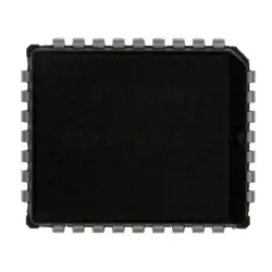
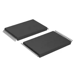
이미지는 참조용만
S34ML16G202BHI003
IC FLASH 16GBIT PARALLEL 63BGA
- 제조업체
- Mfr.부분 #S34ML16G202BHI003
- 패키지 63-VFBGA
- 데이터시트
- 재고 있음4601
100% 원래 &새로운
배송 준비 24 시간
365 일 보장
RFQ 및더 많은 할인
사양
| Package | Bulk |
| Series | ML-2 |
| ProductStatus | Obsolete |
| MemoryType | Non-Volatile |
| MemoryFormat | FLASH |
| Technology | FLASH - NAND |
| MemorySize | 16Gb (2G x 8) |
| MemoryInterface | Parallel |
| WriteCycleTime-WordPage | 25ns |
| Voltage-Supply | 2.7V ~ 3.6V |
| OperatingTemperature | -40°C ~ 85°C (TA) |
| MountingType | Surface Mount |
| Package/Case | 63-VFBGA |
개요
Description
Key features include a 1.8V operating voltage, multiple page sizes, and support for advanced error correction codes (ECC) to ensure data integrity. It also includes options for programmable features, enhancing flexibility for different application needs. The S34ML16G202BHI003 is packaged in a compact BGA (Ball Grid Array) format, which supports efficient PCB layout and thermal management, making it suitable for space-constrained environments. Overall, this NAND flash device is ideal for developers looking for reliable, high-capacity storage solutions.
Features
1. Memory Density: 16 Gb (gigabits), providing substantial storage capacity for applications.
2. Interface: Supports a standard SPI (Serial Peripheral Interface), allowing for easy integration with microcontrollers and other digital devices.
3. Operating Voltage: Typically operates at 3.0V to 3.6V, making it suitable for various power-sensitive applications.
4. Data Transfer Speed: High-speed read performance, allowing for efficient data access and retrieval.
5. Endurance: Designed for a high program/erase cycles, making it suitable for applications requiring frequent data updates.
6. Temperature Range: Supports industrial temperature ranges, making it ideal for use in harsh environments.
7. Erase Block Size: Features a flexible erase block size, enhancing data management capabilities.
This device is commonly used in embedded systems, automotive applications, and IoT devices due to its reliability and performance.
Package
Pinout
The primary functions of these pins include:
1. Data I/O Pins: Used for data transfer (D0-D7).
2. Address Pins: For addressing memory locations (A0-A20).
3. Control Pins: Includes commands for reading, writing, and erasing (e.g., WE for Write Enable, RE for Read Enable).
4. Chip Enable: CE# (Chip Enable) to activate the device.
5. Write Protect: WP# pin to protect against accidental writes.
6. Status Register Output: Provides status information during operations.
The device supports the ONFI (Open NAND Flash Interface) specification, allowing for interoperability with various controllers.
Manufacturer
Application
Equivalent
배송
배송 방법We
DHL, FedEx, TNT, UPS 또는 선택한 다른 운송업체를 통해 글로벌 배송 서비스를 제공합니다.
배송 요금 참조 (DHL/FedEx):
DHL은: 배송 비용은 $25-$45 (0.5kg)에서 2-5 영업일의 추정적 배달 시간이 있습니다.
FedEx는: 배송 비용은 $25-$40 (0.5kg)에서 3-7 영업일의 추정적 배달 시간을 가지고 있습니다.
UPS는: 배송 비용은 $25-$45 (0.5kg)에서 3-7 영업일의 추정적 배달 시간을 가지고 있습니다.
TNT는: 배송 비용은 $25-$65 (0.5kg)에서 3-7 영업일의 추정적 배달 시간을 가지고 있습니다.
EMS는: 배송 비용은 $30-$50 (0.5kg)에서 7-15 영업일의 추정적 배달 시간을 제공합니다.
등록된 항공우편: 배송 비용은 $2-$4 (0.1kg), 예상 배달 시간 5-20 영업일.
지불
Payment Methods
지불 기간은 100% 사전 지불입니다.
현재, 우리는 아래 지불 방법만 받아들입니다.:
1. PayPal
2. 신용/직불 카드
3. 전선 전송
비슷한
-
![MX25R8035FM1IL0]() MX25R8035FM1IL0
Macronix
-
![MX25V1635FZNI]() MX25V1635FZNI
Macronix
-
![MX29F400CBTI-70G]() MX29F400CBTI-70G
Macronix
-
![MX25V16066M1I02]() MX25V16066M1I02
Macronix
-
![MX25L25673GMI-08G]() MX25L25673GMI-08G
Macronix
-
![MX25U51279GXDR00]() MX25U51279GXDR00
Macronix
-
![MX25L6433FM2I-08G]() MX25L6433FM2I-08G
Macronix
-
![MX25L12833FZ2I-10G]() MX25L12833FZ2I-10..
Macronix
-
![MX25L12835FZ2I-10G]() MX25L12835FZ2I-10..
Macronix
-
![MX29F040CQI-70G]() MX29F040CQI-70G
Macronix
-
![MX29F040CTI-70G]() MX29F040CTI-70G
Macronix
-
![MX25U51245GZ4I00]() MX25U51245GZ4I00
Macronix