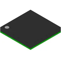
이미지는 참조용만
SN74AUP1T97DSFR
IC XLTR VL UNIDIR 6-SON
- 제조업체
- Mfr.부분 #SN74AUP1T97DSFR
- 패키지
- 데이터시트 SN74AUP1T97DSFR DataSheet
- 재고 있음2031
100% 원래 &새로운
배송 준비 24 시간
365 일 보장
RFQ 및더 많은 할인
사양
| Series | 74AUP |
| Part Status | Active |
| Translator Type | Voltage Level |
| Channel Type | Unidirectional |
| Number of Circuits | 1 |
| Channels per Circuit | 1 |
| Voltage - VCCA | 1.8 V ~ 2.7 V |
| Voltage - VCCB | 2.3 V ~ 3.6 V |
| Output Type | Single-Ended |
| Operating Temperature | -40°C ~ 85°C (TA) |
| Features | Configurable Gate Logic Functions |
| Mounting Type | Surface Mount |
| Package / Case | 6-XFDFN |
| Supplier Device Package | 6-SON (1x1) |
| Base Product Number | 74AUP1T97 |
개요
Description
The Schmitt-trigger input provides noise immunity and ensures clean transitions between logic levels, making it ideal for applications requiring signal conditioning. The device is characterized by a fast propagation delay, typically in the range of 3-5 nanoseconds, which enhances performance in high-speed circuits.
Packaged in a small, space-efficient SOT-23 format, the SN74AUP1T97DSFR is often used in digital logic applications, level shifting, and signal buffering. Its combination of low power consumption, compact size, and reliable operation makes it a popular choice in modern electronic designs.
Features
1. Wide Supply Voltage Range: Operates from 0.8V to 3.6V, allowing flexibility in various applications.
2. Low Power Consumption: Designed for low power usage, making it suitable for battery-powered devices.
3. High Speed: Capable of operating at high frequencies, enabling fast signal processing.
4. Schmitt-Trigger Input: Provides hysteresis for improved noise immunity and cleaner signal transitions.
5. Single Output: This device features one output that can drive standard CMOS loads.
6. Compatible with Logic Levels: Accepts both TTL and CMOS input levels, enhancing versatility.
7. LVCMOS Compatible: Suitable for use in low voltage CMOS applications.
8. Small Package Size: Available in a small form factor (DSBGA package), ideal for space-constrained designs.
These features make the SN74AUP1T97DSFR suitable for a wide range of digital applications, including data communication and signal conditioning.
Package
Pinout
Pin Functions:
1. VCC (Pin 1): Power supply voltage.
2. GND (Pin 2): Ground.
3. A (Pin 3): Input for the signal to be buffered.
4. Y (Pin 4): Output that reflects the input signal with Schmitt-trigger characteristics.
5. OE (Pin 5): Output enable pin; when high, it enables the output (Y); when low, it disables the output.
The device is designed to operate at low voltage levels and features a high input impedance, making it suitable for interfacing with various digital circuits.
Manufacturer
Application
Equivalent
배송
배송 방법We
DHL, FedEx, TNT, UPS 또는 선택한 다른 운송업체를 통해 글로벌 배송 서비스를 제공합니다.
배송 요금 참조 (DHL/FedEx):
DHL은: 배송 비용은 $25-$45 (0.5kg)에서 2-5 영업일의 추정적 배달 시간이 있습니다.
FedEx는: 배송 비용은 $25-$40 (0.5kg)에서 3-7 영업일의 추정적 배달 시간을 가지고 있습니다.
UPS는: 배송 비용은 $25-$45 (0.5kg)에서 3-7 영업일의 추정적 배달 시간을 가지고 있습니다.
TNT는: 배송 비용은 $25-$65 (0.5kg)에서 3-7 영업일의 추정적 배달 시간을 가지고 있습니다.
EMS는: 배송 비용은 $30-$50 (0.5kg)에서 7-15 영업일의 추정적 배달 시간을 제공합니다.
등록된 항공우편: 배송 비용은 $2-$4 (0.1kg), 예상 배달 시간 5-20 영업일.
지불
Payment Methods
지불 기간은 100% 사전 지불입니다.
현재, 우리는 아래 지불 방법만 받아들입니다.:
1. PayPal
2. 신용/직불 카드
3. 전선 전송
비슷한
-
![MX25R3235FZNIL0]() MX25R3235FZNIL0
Macronix
-
![MX25V16066M2I02]() MX25V16066M2I02
Macronix
-
![MX25L25673GMI-08G]() MX25L25673GMI-08G
Macronix
-
![MX25L25673GMI-10G]() MX25L25673GMI-10G
Macronix
-
![MX29GL512FHXFI-11G]() MX29GL512FHXFI-11..
Macronix
-
![MX25L6433FM2I-08G]() MX25L6433FM2I-08G
Macronix
-
![MX25L12833FM2I-10G]() MX25L12833FM2I-10..
Macronix
-
![MX25L12835FZ2I-10G]() MX25L12835FZ2I-10..
Macronix
-
![MX25U51245GZ4I00]() MX25U51245GZ4I00
Macronix
-
![MX25V8035FM2I]() MX25V8035FM2I
Macronix
-
![MX25L6473FM2I-08G]() MX25L6473FM2I-08G
Macronix
-
![MX25L12872FM2I-10G]() MX25L12872FM2I-10..
Macronix