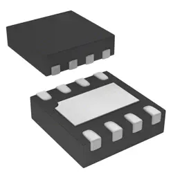
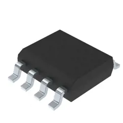
이미지는 참조용만
TEA1795T/N1
NXP Semiconductors TEA1795T/SO8//N1/REEL 13 Q1/T1 *STANDARD MARK SMD
- 제조업체
- Mfr.부분 #TEA1795T/N1
- 패키지
- 데이터시트
- 재고 있음17088
100% 원래 &새로운
배송 준비 24 시간
365 일 보장
RFQ 및더 많은 할인
사양
개요
Description
Key features of the TEA1795T/N1 include a wide input voltage range, enabling operation from universal AC mains, and advanced protection mechanisms such as over-voltage, under-voltage, and over-temperature protection. It also incorporates a frequency jittering function to reduce electromagnetic interference (EMI), enhancing compliance with regulatory standards.
The device utilizes a quasi-resonant switching technique, which improves efficiency by minimizing switching losses, particularly under light load conditions. Additionally, its integrated PWM controller allows for precise regulation of output voltage and current, contributing to reliable performance.
Overall, the TEA1795T/N1 is an efficient and versatile solution for developing compact and reliable power supply systems.
Features
1. Wide Input Voltage Range: Supports universal input voltages (85 to 265 VAC).
2. High Efficiency: Optimized for low standby power consumption and enhanced efficiency.
3. Integrated Startup Circuit: Eliminates the need for external components, simplifying designs.
4. Adjustable Output Voltage: Allows customization of output voltage through an external resistor divider.
5. Protection Features: Includes overvoltage protection (OVP), overcurrent protection (OCP), and thermal protection (OTP).
6. PWM Control: Operates in both continuous and discontinuous conduction modes to improve regulation.
7. Frequency Jittering: Reduces electromagnetic interference (EMI) for compliance with regulations.
8. Low-Demand Features: Built-in features for minimal power loss in idle modes.
These features make the TEA1795T/N1 suitable for applications like chargers, adapters, and power supplies for consumer electronics.
Package
Pinout
### Pin Count and Functions:
1. Pin 1 (CSN): Current sense negative input.
2. Pin 2 (CSN): Current sense positive input.
3. Pin 3 (VDD): Supply voltage input.
4. Pin 4 (GND): Ground.
5. Pin 5 (COMP): Compensation pin for feedback loop.
6. Pin 6 (FB): Feedback input for voltage regulation.
7. Pin 7 (SW): Switch node for external components.
8. Pin 8 (PWM): PWM dimming control input.
9. Pin 9 (VREF): Reference voltage output.
10. Pin 10 (RAMP): Ramp generator control.
11. Pin 11 (DTC): Dimming time control.
12. Pin 12 (RT/CT): Timing resistor/capacitor connection.
13. Pin 13 (SENSE): Current sense for overcurrent protection.
14. Pin 14 (NC): No connection.
15. Pin 15 (DRAIN): External power switch connection.
16. Pin 16 (OUT): Output for driving LED load.
This device is primarily used in LED drivers, providing features such as dimming and current regulation.
Manufacturer
Application
Equivalent
배송
배송 방법We
DHL, FedEx, TNT, UPS 또는 선택한 다른 운송업체를 통해 글로벌 배송 서비스를 제공합니다.
배송 요금 참조 (DHL/FedEx):
DHL은: 배송 비용은 $25-$45 (0.5kg)에서 2-5 영업일의 추정적 배달 시간이 있습니다.
FedEx는: 배송 비용은 $25-$40 (0.5kg)에서 3-7 영업일의 추정적 배달 시간을 가지고 있습니다.
UPS는: 배송 비용은 $25-$45 (0.5kg)에서 3-7 영업일의 추정적 배달 시간을 가지고 있습니다.
TNT는: 배송 비용은 $25-$65 (0.5kg)에서 3-7 영업일의 추정적 배달 시간을 가지고 있습니다.
EMS는: 배송 비용은 $30-$50 (0.5kg)에서 7-15 영업일의 추정적 배달 시간을 제공합니다.
등록된 항공우편: 배송 비용은 $2-$4 (0.1kg), 예상 배달 시간 5-20 영업일.
지불
Payment Methods
지불 기간은 100% 사전 지불입니다.
현재, 우리는 아래 지불 방법만 받아들입니다.:
1. PayPal
2. 신용/직불 카드
3. 전선 전송
비슷한
-
![MX25L3233FZBI-08Q]() MX25L3233FZBI-08Q
Macronix
-
![MX25L3233FM1I-08Q]() MX25L3233FM1I-08Q
Macronix
-
![MX25V1635FZNI]() MX25V1635FZNI
Macronix
-
![MX25V1635FZNQ03]() MX25V1635FZNQ03
Macronix
-
![MX29F400CBTI-70G]() MX29F400CBTI-70G
Macronix
-
![MX25R3235FZNIL0]() MX25R3235FZNIL0
Macronix
-
![MX25L8035EM2I-10G]() MX25L8035EM2I-10G
Macronix
-
![MX25L2006EM1I-12G]() MX25L2006EM1I-12G
Macronix
-
![MX25R1635FZUIH0]() MX25R1635FZUIH0
Macronix
-
![MX25V1635FM2I]() MX25V1635FM2I
Macronix
-
![MX25U25645GXDI00]() MX25U25645GXDI00
Macronix
-
![MX25L25645GXDI-08G]() MX25L25645GXDI-08..
Macronix