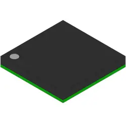
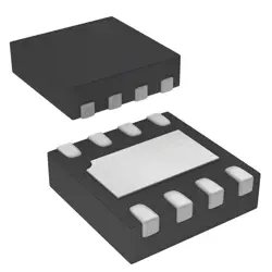
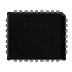
이미지는 참조용만
TPS22950CDDCR
5.5-V, 2-A, 40-M LOAD SWITCH WIT
- 제조업체
- Mfr.부분 #TPS22950CDDCR
- 패키지
- 데이터시트 TPS22950CDDCR DataSheet
- 재고 있음4824
100% 원래 &새로운
배송 준비 24 시간
365 일 보장
RFQ 및더 많은 할인
사양
| Part Status | Active |
개요
Description
The TPS22950 incorporates built-in features such as controlled rise and fall times, which help reduce inrush current and improve system reliability. Additionally, it includes thermal shutdown and over-current protection mechanisms to safeguard the device and connected loads. The device is housed in a compact 2mm x 2mm VQFN package, making it suitable for space-constrained designs.
It is widely used in applications like battery-powered devices, portable electronics, and power distribution networks, where efficient power control and management are critical. Overall, the TPS22950CDDCR is an excellent choice for implementing reliable load-switching solutions in modern electronic systems.
Features
1. Low On-Resistance: It offers a low on-resistance (RDS(ON)) of approximately 16 mΩ, facilitating efficient power delivery with minimal voltage drop.
2. Input Voltage Range: Supports an input voltage range from 1.2V to 5.5V, making it versatile for various applications.
3. High Current Capability: Can handle up to 5A of continuous load current, suitable for powering high-demand devices.
4. Controlled Rise/Fall Times: Adjustable rise (typical 0.5 ms) and fall times help reduce inrush current and EMI.
5. Enable Function: Features an active high enable pin for easy control of the load switch.
6. Thermal Protection: Integrated thermal shutdown ensures device reliability under overheating conditions.
7. Compact Package: Available in a small 4mm x 3mm VQFN package, ideal for space-constrained designs.
These features make the TPS22950CDDCR a reliable choice for managing power in various electronic systems.
Package
Pinout
1. IN (Pin 1): Power input; where the input voltage is supplied.
2. GND (Pin 2): Ground reference; common return path for the circuit.
3. ON (Pin 3): Enable control; a logic high turns on the switch, while a logic low turns it off.
4. OUT (Pin 4): Power output; where the switched output voltage is delivered to the load.
5. SW (Pin 5): This pin is connected to the source of the internal MOSFET switch and is used for monitoring purposes.
6. NC (Pin 6): No connect; not internally connected and can be left unconnected.
The device is designed for low on-resistance and quick turn-on times, making it suitable for power management applications.
Manufacturer
Application
1. Power management in portable devices.
2. Battery-operated equipment to control power distribution.
3. Consumer electronics for power rail sequencing.
4. Automotive systems for load isolation.
5. Telecommunications equipment for energy efficiency.
6. Industrial automation for controlling power to machinery.
Its low on-resistance and fast switching capabilities make it suitable for these applications.
Equivalent
배송
배송 방법We
DHL, FedEx, TNT, UPS 또는 선택한 다른 운송업체를 통해 글로벌 배송 서비스를 제공합니다.
배송 요금 참조 (DHL/FedEx):
DHL은: 배송 비용은 $25-$45 (0.5kg)에서 2-5 영업일의 추정적 배달 시간이 있습니다.
FedEx는: 배송 비용은 $25-$40 (0.5kg)에서 3-7 영업일의 추정적 배달 시간을 가지고 있습니다.
UPS는: 배송 비용은 $25-$45 (0.5kg)에서 3-7 영업일의 추정적 배달 시간을 가지고 있습니다.
TNT는: 배송 비용은 $25-$65 (0.5kg)에서 3-7 영업일의 추정적 배달 시간을 가지고 있습니다.
EMS는: 배송 비용은 $30-$50 (0.5kg)에서 7-15 영업일의 추정적 배달 시간을 제공합니다.
등록된 항공우편: 배송 비용은 $2-$4 (0.1kg), 예상 배달 시간 5-20 영업일.
지불
Payment Methods
지불 기간은 100% 사전 지불입니다.
현재, 우리는 아래 지불 방법만 받아들입니다.:
1. PayPal
2. 신용/직불 카드
3. 전선 전송
비슷한
-
![MX25V1635FZNQ03]() MX25V1635FZNQ03
Macronix
-
![MX66U1G45GXDI00]() MX66U1G45GXDI00
Macronix
-
![MX25V5126FM1I]() MX25V5126FM1I
Macronix
-
![MX25R3235FZNIL0]() MX25R3235FZNIL0
Macronix
-
![MX25V16066M2I02]() MX25V16066M2I02
Macronix
-
![MX25R6435FBDIL0]() MX25R6435FBDIL0
Macronix
-
![MX29GL512FHXFI-11G]() MX29GL512FHXFI-11..
Macronix
-
![MX25U3232FZBI02]() MX25U3232FZBI02
Macronix
-
![MX25U6435FM2I-10G]() MX25U6435FM2I-10G
Macronix
-
![MX25U25645GXDI00]() MX25U25645GXDI00
Macronix
-
![MX25L12835FZ2I-10G]() MX25L12835FZ2I-10..
Macronix
-
![MX29F040CQI-70G]() MX29F040CQI-70G
Macronix