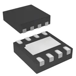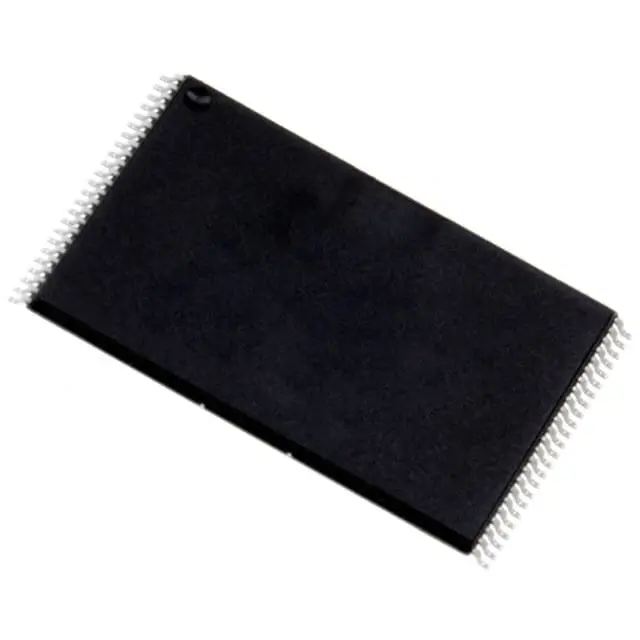
이미지는 참조용만
W29N01GVSIAA
IC FLASH 1GBIT 48-TSOP
- 제조업체
- Mfr.부분 #W29N01GVSIAA
- 패키지
- 데이터시트 W29N01GVSIAA DataSheet
- 재고 있음2801
100% 원래 &새로운
배송 준비 24 시간
365 일 보장
RFQ 및더 많은 할인
사양
| Part Status | Discontinued at DigiKey |
| Base Product Number | W29N01 |
| DigiKey Programmable | Not Verified |
| Memory Type | Non-Volatile |
| Memory Format | FLASH |
| Technology | FLASH - NAND (SLC) |
| Memory Size | 1Gbit |
| Memory Organization | 128M x 8 |
| Write Cycle Time - Word, Page | 25ns |
| Voltage - Supply | 2.7V ~ 3.6V |
| Operating Temperature | -40°C ~ 85°C (TA) |
| Mounting Type | Surface Mount |
| Package | 48-TFSOP (0.724", 18.40mm Width) |
| Supplier Device Package | 48-TSOP |
| Packaging | Tray |
| Access Time | 25 ns |
개요
Description
Key characteristics include a voltage range of 2.7V to 3.6V, ensuring compatibility with most modern microcontrollers. The device is available in various packages, including a compact 8-pin SOP, making it suitable for space-constrained designs. Additionally, it features a page programming mode, which allows for efficient data write operations.
Overall, the W29N01GVSIAA is a reliable choice for applications requiring non-volatile memory with a balance of performance, power efficiency, and compactness.
Features
1. Capacity: 1 Mbit (128 KB) of memory storage.
2. Interface: SPI (Serial Peripheral Interface) for easy integration with microcontrollers.
3. Read Speed: Fast read speeds of up to 104 MHz, enabling efficient data access.
4. Write/Erase Speed: Supports byte-programming and sector-erase capabilities, enhancing data management.
5. Low Power Consumption: Designed for low energy usage, making it ideal for battery-operated devices.
6. Operating Voltage: Typically operates at 2.7V to 3.6V, suitable for wide-ranging applications.
7. Endurance: Offers high endurance with up to 100,000 program/erase cycles per sector.
8. Temperature Range: Available for various temperature ranges, accommodating industrial applications.
These features make the W29N01GVSIAA suitable for applications in consumer electronics, automotive, and IoT devices.
Package
Pinout
### Pin Functions:
1. A0-A25: Address inputs for accessing memory locations.
2. DQ0-DQ7: Data input/output lines for reading and writing data.
3. CE#: Chip Enable; activates the device.
4. OE#: Output Enable; controls data output.
5. WE#: Write Enable; initiates a write operation.
6. RE#: Read Enable; initiates a read operation.
7. RP#: Reset pin; used to reset the device.
8. VCC: Power supply.
9. VSS: Ground.
10. R/B#: Ready/Busy; indicates the status of the device.
11. NC: No Connect; not internally connected.
This device is used in various applications requiring non-volatile memory storage, such as in consumer electronics and embedded systems.
Manufacturer
Application
Equivalent
배송
배송 방법We
DHL, FedEx, TNT, UPS 또는 선택한 다른 운송업체를 통해 글로벌 배송 서비스를 제공합니다.
배송 요금 참조 (DHL/FedEx):
DHL은: 배송 비용은 $25-$45 (0.5kg)에서 2-5 영업일의 추정적 배달 시간이 있습니다.
FedEx는: 배송 비용은 $25-$40 (0.5kg)에서 3-7 영업일의 추정적 배달 시간을 가지고 있습니다.
UPS는: 배송 비용은 $25-$45 (0.5kg)에서 3-7 영업일의 추정적 배달 시간을 가지고 있습니다.
TNT는: 배송 비용은 $25-$65 (0.5kg)에서 3-7 영업일의 추정적 배달 시간을 가지고 있습니다.
EMS는: 배송 비용은 $30-$50 (0.5kg)에서 7-15 영업일의 추정적 배달 시간을 제공합니다.
등록된 항공우편: 배송 비용은 $2-$4 (0.1kg), 예상 배달 시간 5-20 영업일.
지불
Payment Methods
지불 기간은 100% 사전 지불입니다.
현재, 우리는 아래 지불 방법만 받아들입니다.:
1. PayPal
2. 신용/직불 카드
3. 전선 전송
비슷한
-
![MX25L3233FM1I-08Q]() MX25L3233FM1I-08Q
Macronix
-
![MX25V1635FZNI]() MX25V1635FZNI
Macronix
-
![MX29F400CBTI-70G]() MX29F400CBTI-70G
Macronix
-
![MX25V4035FZUI]() MX25V4035FZUI
Macronix
-
![MX25V2033FM1I]() MX25V2033FM1I
Macronix
-
![MX25V16066M2I02]() MX25V16066M2I02
Macronix
-
![MX30LF2G28AD-TI]() MX30LF2G28AD-TI
Macronix
-
![MX25L25673GMI-08G]() MX25L25673GMI-08G
Macronix
-
![MX25U51279GXDR00]() MX25U51279GXDR00
Macronix
-
![MX25U3232FZBI02]() MX25U3232FZBI02
Macronix
-
![MX25L12833FM2I-10G]() MX25L12833FM2I-10..
Macronix
-
![MX25U25645GXDI00]() MX25U25645GXDI00
Macronix