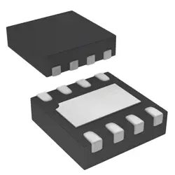
이미지는 참조용만
XC3S4000-5FGG676C
IC FPGA 489 I/O 676FBGA
- 제조업체
- Mfr.부분 #XC3S4000-5FGG676C
- 패키지
- 데이터시트
- 재고 있음9605
100% 원래 &새로운
배송 준비 24 시간
365 일 보장
RFQ 및더 많은 할인
사양
| Series | Spartan®-3 |
| Part Status | Obsolete |
| DigiKey Programmable | Not Verified |
| Number of Logic Elements/Cells | 62208 |
| Total RAM Bits | 1769472 |
| Number of I/O | 489 |
| Voltage - Supply | 1.14V ~ 1.26V |
| Mounting Type | Surface Mount |
| Operating Temperature | 0°C ~ 85°C (TJ) |
| Package / Case | 676-BGA |
| Supplier Device Package | 676-FBGA (27x27) |
| Base Product Number | XC3S4000 |
| Number of LABs/CLBs | 6912 |
| Number of Gates | 4000000 |
개요
Description
Key specifications include:
- Speed Grade: 5, indicating moderate performance.
- Package: FGG676, a fine-pitch ball grid array (FBGA) package with 676 balls for better thermal management and signal integrity.
- I/O Pins: Supports a significant number of user-configurable I/O pins, facilitating integration with various peripherals.
- Power Consumption: Optimized for low power, making it suitable for portable and battery-operated applications.
The XC3S4000 also supports various design tools and languages, including VHDL and Verilog, allowing designers to implement custom logic configurations easily. Its versatility and low cost make it a popular choice for both prototyping and production in the embedded design space.
Features
- Logic Cells: 4,000 configurable logic cells, enabling complex logic implementations.
- I/O Pins: Up to 676 I/O pins, supporting various I/O standards.
- Embedded Block RAM: 144 Kbits of embedded block RAM for efficient data storage.
- Digital Signal Processing (DSP): Capable of supporting basic DSP operations with dedicated resources.
- Speed Grade: -5 speed grade, offering a maximum performance of 150 MHz at 25°C.
- Configuration Options: Multi-boot capability and support for various configuration modes (JTAG, SPI, etc.).
- Power Consumption: Low power usage, suitable for battery-operated and portable applications.
- Development Tools: Compatible with Xilinx ISE design suite for ease of design and implementation.
Overall, the XC3S4000-5FGG676C is designed for applications requiring moderate logic capacity with a balance of performance and power efficiency.
Package
Pinout
The functions of these pins include:
1. I/O Pins: Used for general-purpose input/output, allowing external connections.
2. Power Pins: Provide power supply to the FPGA core and I/O banks.
3. Configuration Pins: Used for configuring the FPGA from external memory or sources.
4. Clock Pins: Dedicated pins for clock signals that drive the internal logic.
5. Ground Pins: Essential for completing electrical circuits and ensuring proper operation.
This FPGA supports a variety of design applications, including digital signal processing, communication, and embedded system designs. The XC3S4000-5 model specifically features a programmable logic capacity of around 4,000 logic cells.
Manufacturer
Application
Equivalent
배송
배송 방법We
DHL, FedEx, TNT, UPS 또는 선택한 다른 운송업체를 통해 글로벌 배송 서비스를 제공합니다.
배송 요금 참조 (DHL/FedEx):
DHL은: 배송 비용은 $25-$45 (0.5kg)에서 2-5 영업일의 추정적 배달 시간이 있습니다.
FedEx는: 배송 비용은 $25-$40 (0.5kg)에서 3-7 영업일의 추정적 배달 시간을 가지고 있습니다.
UPS는: 배송 비용은 $25-$45 (0.5kg)에서 3-7 영업일의 추정적 배달 시간을 가지고 있습니다.
TNT는: 배송 비용은 $25-$65 (0.5kg)에서 3-7 영업일의 추정적 배달 시간을 가지고 있습니다.
EMS는: 배송 비용은 $30-$50 (0.5kg)에서 7-15 영업일의 추정적 배달 시간을 제공합니다.
등록된 항공우편: 배송 비용은 $2-$4 (0.1kg), 예상 배달 시간 5-20 영업일.
지불
Payment Methods
지불 기간은 100% 사전 지불입니다.
현재, 우리는 아래 지불 방법만 받아들입니다.:
1. PayPal
2. 신용/직불 카드
3. 전선 전송
비슷한
-
![MX25V1635FZNQ03]() MX25V1635FZNQ03
Macronix
-
![MX66U1G45GXDI00]() MX66U1G45GXDI00
Macronix
-
![MX25V2033FM1I]() MX25V2033FM1I
Macronix
-
![MX25R3235FZNIL0]() MX25R3235FZNIL0
Macronix
-
![MX30LF2G28AD-TI]() MX30LF2G28AD-TI
Macronix
-
![MX25L8035EM2I-10G]() MX25L8035EM2I-10G
Macronix
-
![MX25U51279GXDR00]() MX25U51279GXDR00
Macronix
-
![MX25L2006EM1I-12G]() MX25L2006EM1I-12G
Macronix
-
![MX25R1635FZUIH0]() MX25R1635FZUIH0
Macronix
-
![MX25V1635FM2I]() MX25V1635FM2I
Macronix
-
![MX25U3232FZBI02]() MX25U3232FZBI02
Macronix
-
![MX25L12833FZ2I-10G]() MX25L12833FZ2I-10..
Macronix