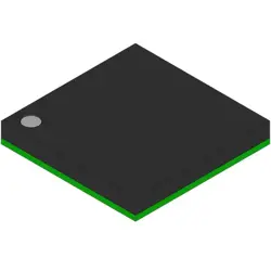
이미지는 참조용만
XC5VSX95T-2FFG1136I
IC FPGA 640 I/O 1136FCBGA
- 제조업체
- Mfr.부분 #XC5VSX95T-2FFG1136I
- 패키지 FBGA-1136
- 데이터시트
- 재고 있음2569
100% 원래 &새로운
배송 준비 24 시간
365 일 보장
RFQ 및더 많은 할인
사양
| Package | Tray |
| Series | Virtex®-5 SXT |
| ProductStatus | Active |
| NumberofLABs/CLBs | 7360 |
| NumberofLogicElements/Cells | 94208 |
| TotalRAMBits | 8994816 |
| NumberofI/O | 640 |
| Voltage-Supply | 0.95V ~ 1.05V |
| MountingType | Surface Mount |
| OperatingTemperature | -40°C ~ 100°C (TJ) |
| Package/Case | 1136-BBGA, FCBGA |
개요
Description
With 1136 pins in a Fine Pitch Ball Grid Array (FBGA) package, it supports a wide range of I/O standards, making it suitable for various interfacing requirements. The XC5VSX95T also incorporates built-in DSP slices for digital signal processing tasks and offers a considerable amount of embedded memory resources.
This FPGA is commonly used in telecommunications, aerospace, defense, and industrial applications due to its reliability and scalability. The programmable nature of FPGAs allows for rapid prototyping and design iterations, making the XC5VSX95T an excellent choice for engineers looking to implement customized hardware solutions. Overall, it's a versatile component for advanced digital design and system integration.
Features
1. Logic Cells: Approximately 95,000 system logic cells, enabling complex designs.
2. DSP Slices: 128 dedicated DSP slices for high-performance signal processing.
3. Block RAM: 4.7 Mbits of distributed Block RAM, providing on-chip memory resources.
4. I/O Pins: Up to 240 user I/O pins, supporting various I/O standards.
5. Clock Management: Integrated clock management with multiple clock inputs and clock dividers.
6. High-Speed Connectivity: Support for advanced serial connectivity protocols such as PCI Express and Gigabit Ethernet.
7. Power Efficiency: Advanced power management features for efficient operation.
The device is ideal for high-performance applications in communications, automotive, aerospace, and industrial control systems, providing flexibility and scalability for complex designs.
Package
Pinout
The FPGA is designed for high-performance applications and includes a variety of resources such as logic cells, DSP slices, and memory blocks. The pins serve multiple functions including:
1. I/O Pins: Configurable for general-purpose input/output (GPIO), supporting various voltage standards.
2. Dedicated Clock Inputs: For clock management and distribution.
3. Configuration Pins: Used for loading the FPGA configuration.
4. Power Pins: For providing the necessary voltage levels to the FPGA.
5. High-Speed Interfaces: Supporting standards like PCIe, SPI, or LVDS, depending on the specific design.
The device is suitable for applications in telecommunications, aerospace, and high-speed data processing.
Manufacturer
Application
Equivalent
- Intel (Altera) Stratix II EP2S180
- Lattice Semiconductor ECP3-70
- Microsemi (Actel) ProASIC3 A3P250
- Xilinx Spartan-6 XC6SLX100
- Xilinx Virtex-6 XC6VSX315.
Ensure to check specifications and compatibility for your specific application.
배송
배송 방법We
DHL, FedEx, TNT, UPS 또는 선택한 다른 운송업체를 통해 글로벌 배송 서비스를 제공합니다.
배송 요금 참조 (DHL/FedEx):
DHL은: 배송 비용은 $25-$45 (0.5kg)에서 2-5 영업일의 추정적 배달 시간이 있습니다.
FedEx는: 배송 비용은 $25-$40 (0.5kg)에서 3-7 영업일의 추정적 배달 시간을 가지고 있습니다.
UPS는: 배송 비용은 $25-$45 (0.5kg)에서 3-7 영업일의 추정적 배달 시간을 가지고 있습니다.
TNT는: 배송 비용은 $25-$65 (0.5kg)에서 3-7 영업일의 추정적 배달 시간을 가지고 있습니다.
EMS는: 배송 비용은 $30-$50 (0.5kg)에서 7-15 영업일의 추정적 배달 시간을 제공합니다.
등록된 항공우편: 배송 비용은 $2-$4 (0.1kg), 예상 배달 시간 5-20 영업일.
지불
Payment Methods
지불 기간은 100% 사전 지불입니다.
현재, 우리는 아래 지불 방법만 받아들입니다.:
1. PayPal
2. 신용/직불 카드
3. 전선 전송
비슷한
-
![MX25L3233FM1I-08Q]() MX25L3233FM1I-08Q
Macronix
-
![MX25V1635FZNQ03]() MX25V1635FZNQ03
Macronix
-
![MX25V5126FM1I]() MX25V5126FM1I
Macronix
-
![MX25V4035FZUI]() MX25V4035FZUI
Macronix
-
![MX25V2033FM1I]() MX25V2033FM1I
Macronix
-
![MX25V16066M1I02]() MX25V16066M1I02
Macronix
-
![MX30LF2G28AD-TI]() MX30LF2G28AD-TI
Macronix
-
![MX29GL512FHXFI-11G]() MX29GL512FHXFI-11..
Macronix
-
![MX25U51279GXDR00]() MX25U51279GXDR00
Macronix
-
![MX25R1635FZUIH0]() MX25R1635FZUIH0
Macronix
-
![MX25V1635FM2I]() MX25V1635FM2I
Macronix
-
![MX25U3232FZBI02]() MX25U3232FZBI02
Macronix