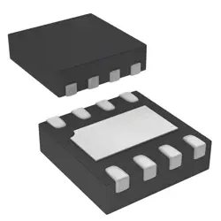
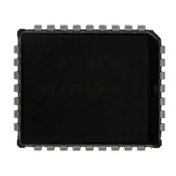
이미지는 참조용만
XC6SLX9-2CSG324I
IC FPGA 200 I/O 324CSBGA
- 제조업체
- Mfr.부분 #XC6SLX9-2CSG324I
- 패키지 BGA-324
- 데이터시트
- 재고 있음6045
100% 원래 &새로운
배송 준비 24 시간
365 일 보장
RFQ 및더 많은 할인
사양
| Package | Tray |
| Series | Spartan®-6 LX |
| ProductStatus | Active |
| NumberofLABs/CLBs | 715 |
| NumberofLogicElements/Cells | 9152 |
| TotalRAMBits | 589824 |
| NumberofI/O | 200 |
| Voltage-Supply | 1.14V ~ 1.26V |
| MountingType | Surface Mount |
| OperatingTemperature | -40°C ~ 100°C (TJ) |
| Package/Case | 324-LFBGA, CSPBGA |
개요
Description
It comes in a CSG324 package, which features 324 pins for flexible connectivity and integration in various designs. The XC6SLX9 includes several key resources such as DSP slices, block RAM, and a rich set of I/O standards, making it suitable for tasks requiring high-speed data processing and efficient resource management.
The "-2" indicates the speed grade, denoting a relatively faster performance within the Spartan-6 family. The device supports a variety of development tools and is compatible with Xilinx's ISE design suite, enabling users to implement complex digital designs efficiently. Overall, the XC6SLX9-2CSG324I is a versatile and cost-effective solution for a broad range of applications.
Features
1. Logic Cells: It offers 9,152 logic cells, enabling complex designs.
2. Registers: Each logic cell includes a configurable register for versatile operations.
3. DSP Slices: Contains 18 DSP slices optimized for digital signal processing tasks.
4. Block RAM: Features 576 Kbits of block RAM for data storage.
5. I/O Pins: Up to 24 differential I/O pairs and multiple LVDS channels for high-speed communication.
6. Speed Grade: Rated at -2, providing a maximum performance of 200 MHz.
7. Power Efficiency: Designed for low power consumption, making it suitable for battery-operated devices.
8. Configuration: Supports multiple configuration modes, including JTAG and SPI.
9. Temperature Range: Ideal for industrial applications with extended temperature ratings.
These attributes make the XC6SLX9-2CSG324I suitable for a variety of applications, including automotive, communications, and consumer electronics.
Package
Pinout
The primary functions of these pins can be categorized as follows:
1. I/O Pins: Configurable for general-purpose input/output, supporting various voltage levels and signaling standards.
2. Power Pins: Dedicated pins for power supply (VCCINT, VCCIO) and ground (GND).
3. Configuration Pins: Pins used for the configuration process, such as the JTAG interface and configuration modes.
4. Clock Pins: Specific pins for clock inputs, which are essential for timing management within the FPGA.
This device is designed for a range of applications, including digital signal processing, communications, and embedded control systems, offering a balance of performance and flexibility in design.
Manufacturer
Application
Equivalent
배송
배송 방법We
DHL, FedEx, TNT, UPS 또는 선택한 다른 운송업체를 통해 글로벌 배송 서비스를 제공합니다.
배송 요금 참조 (DHL/FedEx):
DHL은: 배송 비용은 $25-$45 (0.5kg)에서 2-5 영업일의 추정적 배달 시간이 있습니다.
FedEx는: 배송 비용은 $25-$40 (0.5kg)에서 3-7 영업일의 추정적 배달 시간을 가지고 있습니다.
UPS는: 배송 비용은 $25-$45 (0.5kg)에서 3-7 영업일의 추정적 배달 시간을 가지고 있습니다.
TNT는: 배송 비용은 $25-$65 (0.5kg)에서 3-7 영업일의 추정적 배달 시간을 가지고 있습니다.
EMS는: 배송 비용은 $30-$50 (0.5kg)에서 7-15 영업일의 추정적 배달 시간을 제공합니다.
등록된 항공우편: 배송 비용은 $2-$4 (0.1kg), 예상 배달 시간 5-20 영업일.
지불
Payment Methods
지불 기간은 100% 사전 지불입니다.
현재, 우리는 아래 지불 방법만 받아들입니다.:
1. PayPal
2. 신용/직불 카드
3. 전선 전송
비슷한
-
![MX25L3233FM1I-08Q]() MX25L3233FM1I-08Q
Macronix
-
![MX25V4035FZUI]() MX25V4035FZUI
Macronix
-
![MX25V2033FM1I]() MX25V2033FM1I
Macronix
-
![MX25L8035EM2I-10G]() MX25L8035EM2I-10G
Macronix
-
![MX25L25673GMI-08G]() MX25L25673GMI-08G
Macronix
-
![MX25U51279GXDR00]() MX25U51279GXDR00
Macronix
-
![MX25L2006EM1I-12G]() MX25L2006EM1I-12G
Macronix
-
![MX25U3232FZBI02]() MX25U3232FZBI02
Macronix
-
![MX25L12833FZ2I-10G]() MX25L12833FZ2I-10..
Macronix
-
![MX29F040CQI-70G]() MX29F040CQI-70G
Macronix
-
![MX29F800CBTI-70G]() MX29F800CBTI-70G
Macronix
-
![MX29LV640ETTI-70G]() MX29LV640ETTI-70G
Macronix