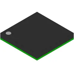
이미지는 참조용만
XC7Z020-1CLG484I
IC SOC CORTEX-A9 667MHZ 484BGA
- 제조업체
- Mfr.부분 #XC7Z020-1CLG484I
- 패키지 CSBGA-484
- 데이터시트
- 재고 있음4498
100% 원래 &새로운
배송 준비 24 시간
365 일 보장
RFQ 및더 많은 할인
사양
| Package | Tray |
| Series | Zynq®-7000 |
| ProductStatus | Active |
| Architecture | MCU, FPGA |
| CoreProcessor | Dual ARM® Cortex®-A9 MPCore™ with CoreSight™ |
| RAMSize | 256KB |
| Peripherals | DMA |
| Connectivity | CANbus, EBI/EMI, Ethernet, I²C, MMC/SD/SDIO, SPI, UART/USART, USB OTG |
| Speed | 667MHz |
| PrimaryAttributes | Artix™-7 FPGA, 85K Logic Cells |
| OperatingTemperature | -40°C ~ 100°C (TJ) |
| Package/Case | 484-LFBGA, CSPBGA |
개요
Description
This device operates at a maximum clock frequency of 1 GHz for the ARM cores and supports multiple interfaces, including Ethernet, USB, and PCIe. The combination of programmable logic and a powerful processing system allows for the development of complex applications that require both high-performance computing and real-time processing capabilities.
The XC7Z020-1CLG484I is packaged in a 484-ball FCG (Fine Pitch Ball Grid Array) format, which facilitates high-density designs. Its programmable nature enables flexibility in hardware configuration, making it ideal for rapid prototyping and development. Overall, the XC7Z020-1CLG484I is a versatile platform for engineers looking to leverage both software and hardware in their designs.
Features
1. Processing System: Dual-core ARM Cortex-A9 (up to 1 GHz), with memory management and various interfaces.
2. FPGA Fabric: 85,000 logic cells, 220 DSP slices, and 4,800 lookup tables (LUTs) for high-performance digital signal processing.
3. Memory Interfaces: Support for DDR3, DDR2, and LPDDR2 memory interfaces, with up to 1,066 MT/s data rates.
4. I/O Connectivity: 54 configurable I/O pins, supporting up to 16 SERDES for high-speed transceivers.
5. Integrated Peripherals: Includes USB, Ethernet, I²C, SPI, UART, and GPIO for versatile connectivity.
6. Low Power: Designed for efficient power consumption, making it suitable for embedded applications.
7. Development Tools: Compatible with Xilinx Vivado Design Suite for HDL and software application development.
This device is widely used in applications like automotive, industrial automation, and communications.
Package
Pinout
Key functions of these pins include:
1. I/O Interfaces: Support for GPIO, I2C, SPI, UART, and other communication protocols.
2. Memory Interfaces: Connections for DDR3/DDR2 memory, including address, data, and control signals.
3. Configuration and JTAG: Pins for device programming and debugging.
4. Power and Ground: Dedicated pins for power supply and ground connections.
5. Clock Inputs: Pins for inputting clock signals for system timing.
The XC7Z020-1CLG484I is commonly used in applications requiring embedded processing combined with high-performance FPGA capabilities.
Manufacturer
Application
Equivalent
1. XC7Z010-1CLG400I - A lower density variant.
2. XC7Z030-1CLG484I - A higher density option.
3. XC7Z020-1CLG484C - A commercial grade version.
4. XC7Z020-1FBG484I - A different package variant.
Always verify compatibility based on specific application requirements.
배송
배송 방법We
DHL, FedEx, TNT, UPS 또는 선택한 다른 운송업체를 통해 글로벌 배송 서비스를 제공합니다.
배송 요금 참조 (DHL/FedEx):
DHL은: 배송 비용은 $25-$45 (0.5kg)에서 2-5 영업일의 추정적 배달 시간이 있습니다.
FedEx는: 배송 비용은 $25-$40 (0.5kg)에서 3-7 영업일의 추정적 배달 시간을 가지고 있습니다.
UPS는: 배송 비용은 $25-$45 (0.5kg)에서 3-7 영업일의 추정적 배달 시간을 가지고 있습니다.
TNT는: 배송 비용은 $25-$65 (0.5kg)에서 3-7 영업일의 추정적 배달 시간을 가지고 있습니다.
EMS는: 배송 비용은 $30-$50 (0.5kg)에서 7-15 영업일의 추정적 배달 시간을 제공합니다.
등록된 항공우편: 배송 비용은 $2-$4 (0.1kg), 예상 배달 시간 5-20 영업일.
지불
Payment Methods
지불 기간은 100% 사전 지불입니다.
현재, 우리는 아래 지불 방법만 받아들입니다.:
1. PayPal
2. 신용/직불 카드
3. 전선 전송
비슷한
-
![MX25R8035FM1IL0]() MX25R8035FM1IL0
Macronix
-
![MX25V1635FZNI]() MX25V1635FZNI
Macronix
-
![MX29F400CBTI-70G]() MX29F400CBTI-70G
Macronix
-
![MX66U1G45GXDI00]() MX66U1G45GXDI00
Macronix
-
![MX25V2033FM1I]() MX25V2033FM1I
Macronix
-
![MX25R3235FZNIL0]() MX25R3235FZNIL0
Macronix
-
![MX30LF2G28AD-TI]() MX30LF2G28AD-TI
Macronix
-
![MX25L25673GMI-08G]() MX25L25673GMI-08G
Macronix
-
![MX29GL512FHXFI-11G]() MX29GL512FHXFI-11..
Macronix
-
![MX25R1635FZUIH0]() MX25R1635FZUIH0
Macronix
-
![MX25L6433FM2I-08G]() MX25L6433FM2I-08G
Macronix
-
![MX25U25645GXDI00]() MX25U25645GXDI00
Macronix