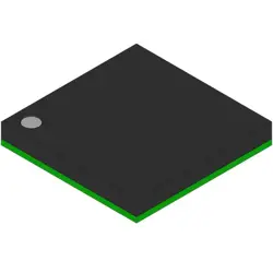
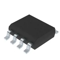
이미지는 참조용만
XCF02S
FPGA - Configuration Memory Flash 2Mb PROM (ST Micro)
- 제조업체
- Mfr.부분 #XCF02S
- 패키지
- 데이터시트
- 재고 있음27839
100% 원래 &새로운
배송 준비 24 시간
365 일 보장
RFQ 및더 많은 할인
사양
| Standard Pack Qty | 74 |
개요
Description
The XCF02S also supports advanced development tools and software ecosystems, enabling developers to easily create, debug, and deploy applications. Its compatibility with popular IDEs and firmware libraries accelerates the development cycle. Additionally, the XCF02S is designed with security features to protect sensitive data, making it a viable choice for IoT and connected devices.
Overall, the XCF02S microcontroller combines performance, versatility, and support, making it an attractive option for developers seeking to build innovative embedded solutions.
Features
1. Architecture: Based on Xilinx's 28nm technology, offering a balance of performance and power efficiency.
2. Logic Cells: It includes a sizable number of configurable logic blocks (CLBs) for versatility in design.
3. I/O Capabilities: Supports multiple I/O standards, enabling integration with various peripherals and systems.
4. Memory Resources: Features embedded block RAM (BRAM) and distributed RAM for efficient data storage and processing.
5. DSP Slices: Contains dedicated digital signal processing (DSP) slices for high-performance arithmetic operations, crucial for applications like signal processing.
6. Configuration Options: Supports multiple configuration methods such as JTAG, SPI, and I2C.
7. Power Management: Offers advanced power-saving features to optimize energy consumption.
8. Development Support: Compatible with Xilinx development tools, facilitating easier design, simulation, and implementation.
These features make the XCF02S suitable for a variety of applications, including communications, automotive, and industrial control.
Package
Pinout
1. VCC - Power supply.
2. GND - Ground connection.
3. SCK (Serial Clock) - Used for clocking data into and out of the device.
4. SI (Serial Input) - Data input pin for programming and configuration.
5. SO (Serial Output) - Data output pin for reading configuration data.
6. CS (Chip Select) - Activates the device for communication.
7. WPN (Write Protect Not) - Used to protect the memory from being written to.
8. WP (Write Protect) - Another pin related to write protection, depending on configuration.
The XCF02S is commonly used for FPGA configuration, enabling efficient programming and reconfiguration in system designs.
Manufacturer
Application
Equivalent
1. Xilinx XC18V02 - A similar EEPROM configuration.
2. Atmel AT17LV01 - A compatible FPGA configuration device.
3. Microchip SST39VF020 - A flash memory alternative.
These components serve similar functions in programming and configuration for FPGAs. Always verify compatibility based on specific application needs.
배송
배송 방법We
DHL, FedEx, TNT, UPS 또는 선택한 다른 운송업체를 통해 글로벌 배송 서비스를 제공합니다.
배송 요금 참조 (DHL/FedEx):
DHL은: 배송 비용은 $25-$45 (0.5kg)에서 2-5 영업일의 추정적 배달 시간이 있습니다.
FedEx는: 배송 비용은 $25-$40 (0.5kg)에서 3-7 영업일의 추정적 배달 시간을 가지고 있습니다.
UPS는: 배송 비용은 $25-$45 (0.5kg)에서 3-7 영업일의 추정적 배달 시간을 가지고 있습니다.
TNT는: 배송 비용은 $25-$65 (0.5kg)에서 3-7 영업일의 추정적 배달 시간을 가지고 있습니다.
EMS는: 배송 비용은 $30-$50 (0.5kg)에서 7-15 영업일의 추정적 배달 시간을 제공합니다.
등록된 항공우편: 배송 비용은 $2-$4 (0.1kg), 예상 배달 시간 5-20 영업일.
지불
Payment Methods
지불 기간은 100% 사전 지불입니다.
현재, 우리는 아래 지불 방법만 받아들입니다.:
1. PayPal
2. 신용/직불 카드
3. 전선 전송
비슷한
-
![MX25R8035FM1IL0]() MX25R8035FM1IL0
Macronix
-
![MX25V1635FZNI]() MX25V1635FZNI
Macronix
-
![MX66U1G45GXDI00]() MX66U1G45GXDI00
Macronix
-
![MX25V4035FZUI]() MX25V4035FZUI
Macronix
-
![MX25V2033FM1I]() MX25V2033FM1I
Macronix
-
![MX25R3235FZNIL0]() MX25R3235FZNIL0
Macronix
-
![MX25V16066M2I02]() MX25V16066M2I02
Macronix
-
![MX29GL512FHXFI-11G]() MX29GL512FHXFI-11..
Macronix
-
![MX25U51279GXDR00]() MX25U51279GXDR00
Macronix
-
![MX25U25643GZNI00]() MX25U25643GZNI00
Macronix
-
![MX25V1635FM2I]() MX25V1635FM2I
Macronix
-
![MX25L6433FM2I-08G]() MX25L6433FM2I-08G
Macronix