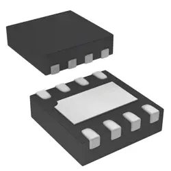
이미지는 참조용만
XCKU11P-2FFVD900I
IC FPGA 408 I/O 900FCBGA
- 제조업체
- Mfr.부분 #XCKU11P-2FFVD900I
- 패키지 FBGA-900
- 데이터시트
- 재고 있음6839
100% 원래 &새로운
배송 준비 24 시간
365 일 보장
RFQ 및더 많은 할인
사양
| Package | Tray |
| Series | Kintex® UltraScale+™ |
| ProductStatus | Active |
| NumberofLABs/CLBs | 37320 |
| NumberofLogicElements/Cells | 653100 |
| TotalRAMBits | 53964800 |
| NumberofI/O | 408 |
| Voltage-Supply | 0.825V ~ 0.876V |
| MountingType | Surface Mount |
| OperatingTemperature | -40°C ~ 100°C (TJ) |
| Package/Case | 900-BBGA, FCBGA |
개요
Description
This FPGA supports advanced features like high-speed serial transceivers, DSP slices for signal processing, and a range of I/O options, making it suitable for applications in telecommunications, automotive, aerospace, and industrial automation. Its architecture enables efficient data handling and processing, allowing for the implementation of algorithms and real-time processing tasks.
Additionally, it offers benefits like low power consumption, scalability, and the ability to adapt to changing requirements, positioning it as a powerful solution for engineers and developers looking to optimize their designs in demanding environments.
Features
1. Architecture: Utilizes a 16nm FinFET process technology for improved performance and power efficiency.
2. Logic Cells: Approximately 110,000 logic cells, providing significant capacity for complex designs.
3. DSP Slices: Includes around 280 DSP slices, optimized for high-speed arithmetic operations, ideal for signal processing applications.
4. Memory: Features integrated block RAM (BRAM) and UltraRAM for efficient data storage and access.
5. I/O Capabilities: Supports high-speed serial transceivers with data rates up to 32.75 Gbps, facilitating high-bandwidth interfaces.
6. Power Efficiency: Designed for low power consumption, making it suitable for embedded and portable applications.
7. Flexible Configuration: Supports various configuration options, including JTAG, SPI, and SelectMAP.
Overall, the XCKU11P-2FFVD900I is a versatile FPGA suited for demanding applications in telecommunications, automotive, and industrial sectors.
Package
Pinout
Manufacturer
Application
Equivalent
1. Xilinx Kintex UltraScale XCKU13P-2FFV900I
2. Xilinx Kintex UltraScale XCKU15P-2FFV900I
3. Intel/Altera Stratix 10 FPGAs (e.g., 10SX220)
4. Lattice Semiconductor ECP5 series
Ensure compatibility in terms of performance, I/O, and application requirements when selecting an equivalent.
배송
배송 방법We
DHL, FedEx, TNT, UPS 또는 선택한 다른 운송업체를 통해 글로벌 배송 서비스를 제공합니다.
배송 요금 참조 (DHL/FedEx):
DHL은: 배송 비용은 $25-$45 (0.5kg)에서 2-5 영업일의 추정적 배달 시간이 있습니다.
FedEx는: 배송 비용은 $25-$40 (0.5kg)에서 3-7 영업일의 추정적 배달 시간을 가지고 있습니다.
UPS는: 배송 비용은 $25-$45 (0.5kg)에서 3-7 영업일의 추정적 배달 시간을 가지고 있습니다.
TNT는: 배송 비용은 $25-$65 (0.5kg)에서 3-7 영업일의 추정적 배달 시간을 가지고 있습니다.
EMS는: 배송 비용은 $30-$50 (0.5kg)에서 7-15 영업일의 추정적 배달 시간을 제공합니다.
등록된 항공우편: 배송 비용은 $2-$4 (0.1kg), 예상 배달 시간 5-20 영업일.
지불
Payment Methods
지불 기간은 100% 사전 지불입니다.
현재, 우리는 아래 지불 방법만 받아들입니다.:
1. PayPal
2. 신용/직불 카드
3. 전선 전송
비슷한
-
![MX25L3233FZBI-08Q]() MX25L3233FZBI-08Q
Macronix
-
![MX25V1635FZNI]() MX25V1635FZNI
Macronix
-
![MX25V2033FM1I]() MX25V2033FM1I
Macronix
-
![MX25V16066M2I02]() MX25V16066M2I02
Macronix
-
![MX30LF2G28AD-TI]() MX30LF2G28AD-TI
Macronix
-
![MX25L8035EM2I-10G]() MX25L8035EM2I-10G
Macronix
-
![MX25U25643GZNI00]() MX25U25643GZNI00
Macronix
-
![MX25V1635FM2I]() MX25V1635FM2I
Macronix
-
![MX25U3232FZBI02]() MX25U3232FZBI02
Macronix
-
![MX25L12833FZ2I-10G]() MX25L12833FZ2I-10..
Macronix
-
![MX25L12833FZNI-10G]() MX25L12833FZNI-10..
Macronix
-
![MX25U25645GXDI00]() MX25U25645GXDI00
Macronix